Welcome to Shenzhen Sing Fung Intelligent Manufacturing Co., Ltd.
E-mail:shaobo@sfi-crf.com
Plasma cleaner manufacturers to share the development of integrated circuits
- Categories:Technical Support
- Author:plasma cleaning machine-surface treatment equipment-CRF plasma machine-Sing Fung Intelligent Manufacturing
- Origin:
- Time of issue:2020-12-23
- Views:
(Summary description)In 1958, the United States, Texas instruments, shows the start of the world's a piece of integrated circuit, wire connect five electronic components in, it marks the world into the era of integrated circuits, from now on, in 1959, Martin @ pull bell LABS (Martin Atalla) and the prosperous khan (Dawon Kahng) developed the first insulated gate field effect transistor (FET) their success factors is by controlling the surface state makes the influence of electric field can penetrate into the semiconductor materials. In studying thermally growing silica, they found that in the structure of the metal layer (M), oxide layer (O insulation), and silicon layer (S semiconductor), these "surface states" are greatly reduced at the junction between silicon and its oxide. In this way, the applied electric field can affect the silicon layer through the oxide layer, hence the name MOS. The research was halted because the original MOS devices were slow and failed to solve the problems faced by telephone devices. But researchers at Fairchild semiconductor and RCA recognize the advantages of MOS devices. In the 1960s, Karl Nininger and Charles Meuller built MOS transistors at Radio Corporation of America. Fairchild semiconductor's C.T.Ah built a MOS tetrode with a control electrode, and MOS transistors began to be used in the development of integrated circuit devices. 1962, Fred heyman (Fred Heiman) and Steven Stan (Steven Hofstein) in the radio corporation of America has made an experimental single chip integrated circuit composed of 16 transistor devices, in 1963, an article written by fairchild with research and development laboratory, along with Frank than lars (Frank Wanlass) in the paper show that, when in connection with complementary symmetry circuit configuration and n - p - channel is the channel of MOS transistor to form the logic circuit (today called CMOS, complementary field effect tube), The power consumption of this circuit is close to zero. This invention was patented by Frank Van Las. CMOS technology laid the foundation for low-power integrated circuits and became the mainstream production technology of digital integrated circuits today. In 1963, in defining and developing standard logic circuits, the transistor-transistor logic (TTL) integrated circuit was established as the standard logic module popular in the 1960s and 1970s due to its advantages in speed, cost and intensity. In 1964, hybrid microcircuits reached their peak production, and the multi-chip SLT packaging technology developed for the IBM Systems /360 computer series entered mass production. In the same year, commercial MOS integrated circuits were introduced, and General Microelectronics used the MOS process to achieve a higher level of integration than bipolar integrated circuits, and used the technology to create an original calculator chipset. In 1968, Federico Faggin and Tom Klein improved the reliability, speed, and package integration of MOS integrated circuits using a silicon gate structure instead of a metal gate. Fagg designed an original commercial silicon gate integrated circuit (Fairchild 3708). In 1971, Intel engineers created the first single-chip microprocessor (CPU), the I4004, to reduce the number of chips needed to design an arithmetic unit. In 1974, the integrated circuit used for LCD digital watches was the original product (SoC) that integrated the entire electronic system onto a single silicon wafer. In 1978, user programmable logic devices (programmable row logic) were born. In order to allow customers to quickly define logic functions, John Birkner and H.T.Cooer of Monocle developed easy-to-use programmable row logic (PAL) devices and software tools. In 1979, the monocle digital signal processor was born. Bell LABS single-chip digital signal processor DSP - 1 device structure makes the electronic switch system more perfect, in the same period, Texas instruments developed in programmable DSP1965 fairchild semiconductor r&d director Gordon Moore (Gordon Moore) had written an internal document, he compiled 5 groups of product development from 1959 to 1964 and with low cost of chip integration and a single device in graphs, then draw a line through these points. From this graph, Gordon Moore found that each new chip contained roughly twice the capacity of its predecessor, and that each new chip was produced within 18-24 months of the previous one. If this trend continues, computing power will rise exponentially relative to the time period. Moore's observation is now known as Moore's law. Over the next decade, he predicted, the number of devices on chips would double every year, reaching 6,500 by 1975. "For integrated circuits, cost-cutting is very attractive," he said. The cost advantage will continue to grow as technology advances to enable the integration of more and more circuit functions on a single chip. In 1975, has joined Intel Gordon M
Plasma cleaner manufacturers to share the development of integrated circuits
(Summary description)In 1958, the United States, Texas instruments, shows the start of the world's a piece of integrated circuit, wire connect five electronic components in, it marks the world into the era of integrated circuits, from now on, in 1959, Martin @ pull bell LABS (Martin Atalla) and the prosperous khan (Dawon Kahng) developed the first insulated gate field effect transistor (FET) their success factors is by controlling the surface state makes the influence of electric field can penetrate into the semiconductor materials. In studying thermally growing silica, they found that in the structure of the metal layer (M), oxide layer (O insulation), and silicon layer (S semiconductor), these "surface states" are greatly reduced at the junction between silicon and its oxide. In this way, the applied electric field can affect the silicon layer through the oxide layer, hence the name MOS. The research was halted because the original MOS devices were slow and failed to solve the problems faced by telephone devices. But researchers at Fairchild semiconductor and RCA recognize the advantages of MOS devices. In the 1960s, Karl Nininger and Charles Meuller built MOS transistors at Radio Corporation of America. Fairchild semiconductor's C.T.Ah built a MOS tetrode with a control electrode, and MOS transistors began to be used in the development of integrated circuit devices.
1962, Fred heyman (Fred Heiman) and Steven Stan (Steven Hofstein) in the radio corporation of America has made an experimental single chip integrated circuit composed of 16 transistor devices, in 1963, an article written by fairchild with research and development laboratory, along with Frank than lars (Frank Wanlass) in the paper show that, when in connection with complementary symmetry circuit configuration and n - p - channel is the channel of MOS transistor to form the logic circuit (today called CMOS, complementary field effect tube), The power consumption of this circuit is close to zero. This invention was patented by Frank Van Las. CMOS technology laid the foundation for low-power integrated circuits and became the mainstream production technology of digital integrated circuits today.
In 1963, in defining and developing standard logic circuits, the transistor-transistor logic (TTL) integrated circuit was established as the standard logic module popular in the 1960s and 1970s due to its advantages in speed, cost and intensity. In 1964, hybrid microcircuits reached their peak production, and the multi-chip SLT packaging technology developed for the IBM Systems /360 computer series entered mass production. In the same year, commercial MOS integrated circuits were introduced, and General Microelectronics used the MOS process to achieve a higher level of integration than bipolar integrated circuits, and used the technology to create an original calculator chipset. In 1968, Federico Faggin and Tom Klein improved the reliability, speed, and package integration of MOS integrated circuits using a silicon gate structure instead of a metal gate. Fagg designed an original commercial silicon gate integrated circuit (Fairchild 3708). In 1971, Intel engineers created the first single-chip microprocessor (CPU), the I4004, to reduce the number of chips needed to design an arithmetic unit. In 1974, the integrated circuit used for LCD digital watches was the original product (SoC) that integrated the entire electronic system onto a single silicon wafer. In 1978, user programmable logic devices (programmable row logic) were born. In order to allow customers to quickly define logic functions, John Birkner and H.T.Cooer of Monocle developed easy-to-use programmable row logic (PAL) devices and software tools. In 1979, the monocle digital signal processor was born.
Bell LABS single-chip digital signal processor DSP - 1 device structure makes the electronic switch system more perfect, in the same period, Texas instruments developed in programmable DSP1965 fairchild semiconductor r&d director Gordon Moore (Gordon Moore) had written an internal document, he compiled 5 groups of product development from 1959 to 1964 and with low cost of chip integration and a single device in graphs, then draw a line through these points. From this graph, Gordon Moore found that each new chip contained roughly twice the capacity of its predecessor, and that each new chip was produced within 18-24 months of the previous one. If this trend continues, computing power will rise exponentially relative to the time period. Moore's observation is now known as Moore's law. Over the next decade, he predicted, the number of devices on chips would double every year, reaching 6,500 by 1975. "For integrated circuits, cost-cutting is very attractive," he said. The cost advantage will continue to grow as technology advances to enable the integration of more and more circuit functions on a single chip. In 1975, has joined Intel Gordon M
- Categories:Technical Support
- Author:plasma cleaning machine-surface treatment equipment-CRF plasma machine-Sing Fung Intelligent Manufacturing
- Origin:
- Time of issue:2020-12-23 11:15
- Views:
Plasma cleaner manufacturers to share the development of integrated circuits:
In 1958, the United States, Texas instruments, shows the start of the world's a piece of integrated circuit, wire connect five electronic components in, it marks the world into the era of integrated circuits, from now on, in 1959, Martin @ pull bell LABS (Martin Atalla) and the prosperous khan (Dawon Kahng) developed the first insulated gate field effect transistor (FET) their success factors is by controlling the surface state makes the influence of electric field can penetrate into the semiconductor materials. In studying thermally growing silica, they found that in the structure of the metal layer (M), oxide layer (O insulation), and silicon layer (S semiconductor), these "surface states" are greatly reduced at the junction between silicon and its oxide. In this way, the applied electric field can affect the silicon layer through the oxide layer, hence the name MOS. The research was halted because the original MOS devices were slow and failed to solve the problems faced by telephone devices. But researchers at Fairchild semiconductor and RCA recognize the advantages of MOS devices. In the 1960s, Karl Nininger and Charles Meuller built MOS transistors at Radio Corporation of America. Fairchild semiconductor's C.T.Ah built a MOS tetrode with a control electrode, and MOS transistors began to be used in the development of integrated circuit devices.
1962, Fred heyman (Fred Heiman) and Steven Stan (Steven Hofstein) in the radio corporation of America has made an experimental single chip integrated circuit composed of 16 transistor devices, in 1963, an article written by fairchild with research and development laboratory, along with Frank than lars (Frank Wanlass) in the paper show that, when in connection with complementary symmetry circuit configuration and n - p - channel is the channel of MOS transistor to form the logic circuit (today called CMOS, complementary field effect tube), The power consumption of this circuit is close to zero. This invention was patented by Frank Van Las. CMOS technology laid the foundation for low-power integrated circuits and became the mainstream production technology of digital integrated circuits today.
In 1963, in defining and developing standard logic circuits, the transistor-transistor logic (TTL) integrated circuit was established as the standard logic module popular in the 1960s and 1970s due to its advantages in speed, cost and intensity. In 1964, hybrid microcircuits reached their peak production, and the multi-chip SLT packaging technology developed for the IBM Systems /360 computer series entered mass production. In the same year, commercial MOS integrated circuits were introduced, and General Microelectronics used the MOS process to achieve a higher level of integration than bipolar integrated circuits, and used the technology to create an original calculator chipset. In 1968, Federico Faggin and Tom Klein improved the reliability, speed, and package integration of MOS integrated circuits using a silicon gate structure instead of a metal gate. Fagg designed an original commercial silicon gate integrated circuit (Fairchild 3708). In 1971, Intel engineers created the first single-chip microprocessor (CPU), the I4004, to reduce the number of chips needed to design an arithmetic unit. In 1974, the integrated circuit used for LCD digital watches was the original product (SoC) that integrated the entire electronic system onto a single silicon wafer. In 1978, user programmable logic devices (programmable row logic) were born. In order to allow customers to quickly define logic functions, John Birkner and H.T.Cooer of Monocle developed easy-to-use programmable row logic (PAL) devices and software tools. In 1979, the monocle digital signal processor was born.
Bell LABS single-chip digital signal processor DSP - 1 device structure makes the electronic switch system more perfect, in the same period, Texas instruments developed in programmable DSP1965 fairchild semiconductor r&d director Gordon Moore (Gordon Moore) had written an internal document, he compiled 5 groups of product development from 1959 to 1964 and with low cost of chip integration and a single device in graphs, then draw a line through these points. From this graph, Gordon Moore found that each new chip contained roughly twice the capacity of its predecessor, and that each new chip was produced within 18-24 months of the previous one. If this trend continues, computing power will rise exponentially relative to the time period. Moore's observation is now known as Moore's law. Over the next decade, he predicted, the number of devices on chips would double every year, reaching 6,500 by 1975. "For integrated circuits, cost-cutting is very attractive," he said. The cost advantage will continue to grow as technology advances to enable the integration of more and more circuit functions on a single chip. In 1975, has joined Intel Gordon Moore's law on his own "made a change, and points out that the number of transistors chip integration will double every two years advanced integrated circuit is the microprocessor or multi-core processor" core "(cores), can control everything from computers to mobile phones and other digital products.
Memory and ASICS are examples of other families of integrated circuits that are important to the modern information society. Although the cost of designing and developing a complex integrated circuit is very high, the cost per IC can be significantly reduced when spread over products that are typically millions of dollars. The PERFORMANCE of IC is high because the small size leads to short paths, allowing low power logic circuits to be applied at fast switching speeds. In recent years, as IC's have continued to grow to smaller dimensions, each chip can encapsulate many circuits. This not only increases the capacity per unit area, but also reduces the cost and increases the function. In conclusion, with the reduction of the shape scale, almost all indicators have been improved, unit cost and switching power consumption have been reduced, and speed has been improved. However, with the scale shrinking, the device's leakage current will also increase. Therefore, the speed and power consumption of users will increase significantly, so manufacturers need to use better graphics design and process optimization to meet such a severe challenge. It is well described in the International TechnologyRoadmap for Semiconductors (ITRS). The evolution of Intel series processors in semiconductor manufacturing technology in the past 15 years, from 130nm silicon gate to 65mm silicon gate manufacturing technology, and then to 32nm metal gate manufacturing technology, now the new fin-type fET metal gate processor has reached the peak of semiconductor manufacturing.
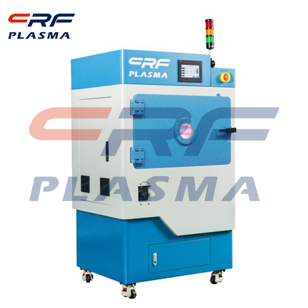
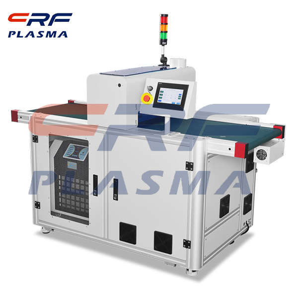
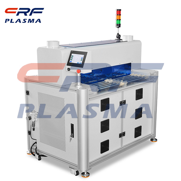
Compared with the traditional planar transistor, FINFET adopts three-dimensional structure and greatly increases the control area of the gate stage, so it can greatly shorten the length of the transistor, reduce leakage current and reduce the short channel effect caused by the scale minification. Intel introduced the commercial FINFET with 22nm node process in 2011: At the end of 2014, Samsung realized the mass production of 14nm FINFET process to provide faster and more power-saving processors for future mobile communication devices. TSMC followed suit in 2015 with the enhanced 16 nm FINFET+. At present, The processors of Apple's high-end mobile phones iphone7 and iphone7 Plus respectively adopt the industry mainstream FINFEI technology, and high-end mobile chips such as Kirin 950 developed by China Sea Technology also adopt FINFET technology. In the process of logic circuit, the etching of the front section of the logical plasma cleaning machine focuses on the construction of the field effect tube, while the etching of the back section of the plasma cleaning machine focuses on the circuit connection.

Scan the QR code to read on your phone

TEL:0755-3367 3020 / 0755-3367 3019

E-mail:sales-sfi@sfi-crf.com

ADD:Mabao Industrial Zone, Huangpu, Baoan District, Shenzhen


