

Welcome to Shenzhen Sing Fung Intelligent Manufacturing Co., Ltd.
E-mail:shaobo@sfi-crf.com


Semiconductor chip industry
- Categories:Semiconductor packaging industry
- Author:
- Origin:
- Time of issue:2020-06-10
- Views:
(Summary description)The bonding between the chip and the package substrate is often two materials with different properties. The surface of the material is usually hydrophobic and inert, and its surface bonding performance is poor. The interface is prone to voids during the bonding process. After sealing and packaging The chip brings great hidden dangers. Plasma treatment on the surface of the chip and the package substrate can effectively increase the surface activity, greatly improve the fluidity of the bonding epoxy resin on the surface, and improve the adhesion of the chip and the package substrate. Junction wettability reduces the delamination between the chip and the substrate, improves the thermal conductivity, improves the reliability and stability of the IC package, and increases the life of the product.

Semiconductor chip industry
(Summary description)The bonding between the chip and the package substrate is often two materials with different properties. The surface of the material is usually hydrophobic and inert, and its surface bonding performance is poor. The interface is prone to voids during the bonding process. After sealing and packaging The chip brings great hidden dangers. Plasma treatment on the surface of the chip and the package substrate can effectively increase the surface activity, greatly improve the fluidity of the bonding epoxy resin on the surface, and improve the adhesion of the chip and the package substrate. Junction wettability reduces the delamination between the chip and the substrate, improves the thermal conductivity, improves the reliability and stability of the IC package, and increases the life of the product.
- Categories:Semiconductor packaging industry
- Author:
- Origin:
- Time of issue:2020-06-10 14:13
- Views:
Information
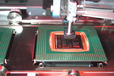
Pre-treatment for die attach
The bonding between the chip and the package substrate is often two materials with different properties. The surface of the material is usually hydrophobic and inert, and its surface bonding performance is poor. The interface is prone to voids during the bonding process. After sealing and packaging The chip brings great hidden dangers. Plasma treatment on the surface of the chip and the package substrate can effectively increase the surface activity, greatly improve the fluidity of the bonding epoxy resin on the surface, and improve the adhesion of the chip and the package substrate. Junction wettability reduces the delamination between the chip and the substrate, improves the thermal conductivity, improves the reliability and stability of the IC package, and increases the life of the product.
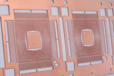
Surface treatment of lead frame
In the field of microelectronics packaging, the plastic packaging form of the lead frame is still used, which still accounts for 80%. It mainly uses copper alloy materials with good thermal conductivity, electrical conductivity and good processing performance as the lead frame copper oxide and other organic pollutants. It causes the delamination between the sealing mold and the copper lead frame, resulting in poor sealing performance and chronic gas leakage after packaging, and also affects the bonding and wire bonding quality of the chip. To ensure the ultra-clean lead frame is to ensure the reliability of the package The key to yield is that plasma treatment can achieve the effect of ultra-purification and activation of the lead frame surface. The yield of the finished product is greatly improved compared with traditional wet cleaning, and it eliminates waste water discharge and reduces the cost of chemical medicine procurement.
Optimize wire bonding (wire bonding)
The quality of the integrated circuit wire bonder has a decisive influence on the reliability of the microelectronic device. The bonding area must be free of contaminants and have good bonding characteristics. The presence of contaminants, such as chlorides and organic residues, will severely weaken the pull value of the wire bond pad. The traditional wet cleaning does not completely remove or cannot remove the contaminants in the bonding area. Plasma cleaning can effectively remove the surface contamination of the bonding area and activate the surface, which can significantly improve the bonding tension of the wire. Greatly improve the reliability of packaged devices.
Scan the QR code to read on your phone
Previous:
None
Next:
None
Previous:
None
Next:
None


TEL:0755-3367 3020 / 0755-3367 3019

E-mail:sales-sfi@sfi-crf.com

ADD:Mabao Industrial Zone, Huangpu, Baoan District, Shenzhen

