

Welcome to Shenzhen Sing Fung Intelligent Manufacturing Co., Ltd.
E-mail:shaobo@sfi-crf.com


News
What are the characteristics and industry applications of the wide linear plasma cleaner
- Categories:Industry News
- Author:Plasma cleaning machine-CRF plasma plasma equipment-plasma surface treatment machine manufacturer-chengfeng intelligent manufacturing
- Origin:
- Time of issue:2021-11-25
- Views:
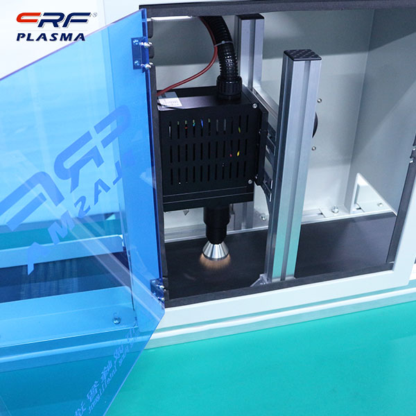
(Summary description)What are the characteristics and industry applications of the wide linear plasma cleaner: The wide linear plasma cleaner is one of the high-power plasma processor control systems, which includes touch screen + PLC automatic control + high-power plasma generator, the air intake system 2-5 working gas options: Ar2, N2, H2, CF4, O2. The characteristics of the wide-width linear plasma cleaner: high precision, fast response, controllability, good compatibility, complete functions, and professionalism. Widely used in: printed circuit board industry, semiconductor IC field, silica gel, plastics, polymers, automotive electronics, aviation industry and other fields. Printed circuit board industry: high-frequency circuit board surface activation, multi-layer circuit board surface cleaning, de-drilling pollution, soft and hard combined circuit board surface cleaning, de-drilling pollution, activation before soft board reinforcement. Semiconductor IC field: COB, COG, COF, ACF process, suitable for wire cleaning before and during welding. Silica gel, plastics, and polymers: the surface roughening, etching and activation of silica gel, plastics, and polymers; the wide linear plasma cleaner PTLplasma cleaning method can be used to change the surface characteristics of BGA organic substrates. Cleaned the liquid crystal display device: the ITO electrode, after the ITO electrode is cleaned, the bonding strength of the ACF is improved. Cleaning COF (ILB) bonding surface: cleaning all parts of the film substrate bonded with the chip (Chip). Cleaning the OLB (FOG) interface surface: cleaning the interface surface between the LCD/PDP panel and the film substrate. Clean the COG: clean the driver IC directly before mounting it on the glass substrate. Cleaning the film substrate: remove organic contaminants attached to the film substrate. Cleaning the metal substrate: remove the attached organic contaminants on the connection part to improve the shear strength of the sealing resin. The photosensitive film of the chip: The photosensitive film (protective film) on the chip is removed by the plasma method of a wide-format linear plasma cleaner. Cleaning the BGA substrate and bonding pad: Clean the bonding pad with a wide-width linear plasma cleaner to improve the lead adhesion and the shear peel strength of the sealing resin. Clean CPS: Remove organic contaminants on the contact surface of the chip and CSP solder balls. Clean the combined chip packaging: clean the contact parts of the composite electronic components.
What are the characteristics and industry applications of the wide linear plasma cleaner
(Summary description)What are the characteristics and industry applications of the wide linear plasma cleaner:
The wide linear plasma cleaner is one of the high-power plasma processor control systems, which includes touch screen + PLC automatic control + high-power plasma generator, the air intake system 2-5 working gas options: Ar2, N2, H2, CF4, O2.
The characteristics of the wide-width linear plasma cleaner: high precision, fast response, controllability, good compatibility, complete functions, and professionalism. Widely used in: printed circuit board industry, semiconductor IC field, silica gel, plastics, polymers, automotive electronics, aviation industry and other fields.
Printed circuit board industry: high-frequency circuit board surface activation, multi-layer circuit board surface cleaning, de-drilling pollution, soft and hard combined circuit board surface cleaning, de-drilling pollution, activation before soft board reinforcement. Semiconductor IC field: COB, COG, COF, ACF process, suitable for wire cleaning before and during welding.
Silica gel, plastics, and polymers: the surface roughening, etching and activation of silica gel, plastics, and polymers; the wide linear plasma cleaner PTLplasma cleaning method can be used to change the surface characteristics of BGA organic substrates. Cleaned the liquid crystal display device: the ITO electrode, after the ITO electrode is cleaned, the bonding strength of the ACF is improved. Cleaning COF (ILB) bonding surface: cleaning all parts of the film substrate bonded with the chip (Chip).
Cleaning the OLB (FOG) interface surface: cleaning the interface surface between the LCD/PDP panel and the film substrate. Clean the COG: clean the driver IC directly before mounting it on the glass substrate. Cleaning the film substrate: remove organic contaminants attached to the film substrate. Cleaning the metal substrate: remove the attached organic contaminants on the connection part to improve the shear strength of the sealing resin.
The photosensitive film of the chip: The photosensitive film (protective film) on the chip is removed by the plasma method of a wide-format linear plasma cleaner. Cleaning the BGA substrate and bonding pad: Clean the bonding pad with a wide-width linear plasma cleaner to improve the lead adhesion and the shear peel strength of the sealing resin. Clean CPS: Remove organic contaminants on the contact surface of the chip and CSP solder balls. Clean the combined chip packaging: clean the contact parts of the composite electronic components.
- Categories:Industry News
- Author:Plasma cleaning machine-CRF plasma plasma equipment-plasma surface treatment machine manufacturer-chengfeng intelligent manufacturing
- Origin:
- Time of issue:2021-11-25 17:36
- Views:
Information
What are the characteristics and industry applications of the wide linear plasma cleaner:
The wide linear plasma cleaner is one of the high-power plasma processor control systems, which includes touch screen + PLC automatic control + high-power plasma generator, the air intake system 2-5 working gas options: Ar2, N2, H2, CF4, O2.
 The characteristics of the wide-width linear plasma cleaner: high precision, fast response, controllability, good compatibility, complete functions, and professionalism. Widely used in: printed circuit board industry, semiconductor IC field, silica gel, plastics, polymers, automotive electronics, aviation industry and other fields.
Printed circuit board industry: high-frequency circuit board surface activation, multi-layer circuit board surface cleaning, de-drilling pollution, soft and hard combined circuit board surface cleaning, de-drilling pollution, activation before soft board reinforcement. Semiconductor IC field: COB, COG, COF, ACF process, suitable for wire cleaning before and during welding.
Silica gel, plastics, and polymers: the surface roughening, etching and activation of silica gel, plastics, and polymers; the wide linear plasma cleaner PTLplasma cleaning method can be used to change the surface characteristics of BGA organic substrates. Cleaned the liquid crystal display device: the ITO electrode, after the ITO electrode is cleaned, the bonding strength of the ACF is improved. Cleaning COF (ILB) bonding surface: cleaning all parts of the film substrate bonded with the chip (Chip).
Cleaning the OLB (FOG) interface surface: cleaning the interface surface between the LCD/PDP panel and the film substrate. Clean the COG: clean the driver IC directly before mounting it on the glass substrate. Cleaning the film substrate: remove organic contaminants attached to the film substrate. Cleaning the metal substrate: remove the attached organic contaminants on the connection part to improve the shear strength of the sealing resin.
The photosensitive film of the chip: The photosensitive film (protective film) on the chip is removed by the plasma method of a wide-format linear plasma cleaner. Cleaning the BGA substrate and bonding pad: Clean the bonding pad with a wide-width linear plasma cleaner to improve the lead adhesion and the shear peel strength of the sealing resin. Clean CPS: Remove organic contaminants on the contact surface of the chip and CSP solder balls. Clean the combined chip packaging: clean the contact parts of the composite electronic components.
Scan the QR code to read on your phone
Relevant Information

The 6 major treatment effects of surface plasma treatment equipment can be applied to 100+ industries to improve product performance
2021-11-24 17:35

The surface energy tester is a characteristic tester with 5 major structures and 8 major functions
2021-11-23 22:06

What are the advantages of plasma cleaning technology What materials can be processed
2021-11-22 22:04

In 2021, the plasma cleaning machine will sort out 8 questions and answers for customers. Don't miss it
2021-11-21 17:28

Chengfeng Zhizhi plasma surface activation treatment and contact angle test program application
2021-11-20 17:27

Plasma treatment machine to clean the surface can improve the surface tension, bonding modification applications
2021-11-19 18:09

The 5 major pretreatment advantages of plasma treatment machine technology process realize online treatment
2021-11-17 22:14

Application in surface treatment of special plasma equipment for wafer processing by Chengfeng Zhizhi
2021-11-16 22:13

How does the atmospheric rotary plasma cleaning machine distinguish between independent and online equipment
2021-11-15 17:24


TEL:0755-3367 3020 / 0755-3367 3019

E-mail:sales-sfi@sfi-crf.com

ADD:Mabao Industrial Zone, Huangpu, Baoan District, Shenzhen

