

Welcome to Shenzhen Sing Fung Intelligent Manufacturing Co., Ltd.
E-mail:shaobo@sfi-crf.com


News
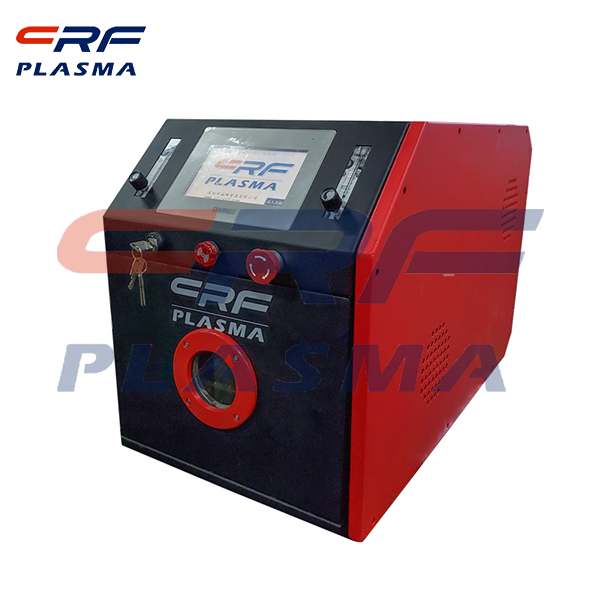
FPC circuit board chip plasma cleaning machine application
- Categories:Industry News
- Author:plasma cleaning machine-surface treatment equipment-CRF plasma machine-Sing Fung Intelligent Manufacturing
- Origin:
- Time of issue:2021-01-21
- Views:
(Summary description)Plasma activation in the electronics industry, cleaning process is the key to reduce the cost, high reliability, process technology, before the chip PCB conductive coating, first plasma activation cleaning processing, fine cleaning and in addition to electrostatic plasma cleaning machine, and guaranteeing the strong adhesion of the coating, the plasma surface cleaning technology in the field of chip packaging, can choose atmospheric pressure or vacuum equipment for processing. One is the plastic window part of the isoionization treatment, due to the use of isoionization treatment technology, so that the surface performance of the material has been improved, so that the coating distribution is more uniform, which not only makes the product looks impeccable, but also greatly reduce the rejection rate in the production process. Application of plasma cleaning machine in FPC circuit board industry: As the substrate of electronic components, printed circuit board has conductivity, which poses a challenge to the use of atmospheric pressure process to treat printed circuit board. Any surface pretreatment method, even if only generates a small potential, may cause short circuit, resulting in wiring and electronic device damage. For this type of electronic application, the special property of plasma cleaning machine processing technology opens up new possibilities for industrial applications in this field. Application of plasma cleaning machine in silicon wafer and chip industry: Silicon wafers, chips and high-performance semiconductors are highly sensitive electronic components, and plasma cleaning machine technology as a manufacturing process is also developing with the development of these technologies. The development of plasma technology in atmospheric environment provides a new application prospect for plasma cleaning, especially plays an important role in automatic production.
FPC circuit board chip plasma cleaning machine application
(Summary description)Plasma activation in the electronics industry, cleaning process is the key to reduce the cost, high reliability, process technology, before the chip PCB conductive coating, first plasma activation cleaning processing, fine cleaning and in addition to electrostatic plasma cleaning machine, and guaranteeing the strong adhesion of the coating, the plasma surface cleaning technology in the field of chip packaging, can choose atmospheric pressure or vacuum equipment for processing. One is the plastic window part of the isoionization treatment, due to the use of isoionization treatment technology, so that the surface performance of the material has been improved, so that the coating distribution is more uniform, which not only makes the product looks impeccable, but also greatly reduce the rejection rate in the production process.
Application of plasma cleaning machine in FPC circuit board industry:
As the substrate of electronic components, printed circuit board has conductivity, which poses a challenge to the use of atmospheric pressure process to treat printed circuit board. Any surface pretreatment method, even if only generates a small potential, may cause short circuit, resulting in wiring and electronic device damage. For this type of electronic application, the special property of plasma cleaning machine processing technology opens up new possibilities for industrial applications in this field.
Application of plasma cleaning machine in silicon wafer and chip industry:
Silicon wafers, chips and high-performance semiconductors are highly sensitive electronic components, and plasma cleaning machine technology as a manufacturing process is also developing with the development of these technologies. The development of plasma technology in atmospheric environment provides a new application prospect for plasma cleaning, especially plays an important role in automatic production.
- Categories:Industry News
- Author:plasma cleaning machine-surface treatment equipment-CRF plasma machine-Sing Fung Intelligent Manufacturing
- Origin:
- Time of issue:2021-01-21 13:42
- Views:
Information
FPC circuit board chip plasma cleaning machine application:
Plasma activation in the electronics industry, cleaning process is the key to reduce the cost, high reliability, process technology, before the chip PCB conductive coating, first plasma activation cleaning processing, fine cleaning and in addition to electrostatic plasma cleaning machine, and guaranteeing the strong adhesion of the coating, the plasma surface cleaning technology in the field of chip packaging, can choose atmospheric pressure or vacuum equipment for processing. One is the plastic window part of the isoionization treatment, due to the use of isoionization treatment technology, so that the surface performance of the material has been improved, so that the coating distribution is more uniform, which not only makes the product looks impeccable, but also greatly reduce the rejection rate in the production process.
Application of plasma cleaning machine in FPC circuit board industry:
As the substrate of electronic components, printed circuit board has conductivity, which poses a challenge to the use of atmospheric pressure process to treat printed circuit board. Any surface pretreatment method, even if only generates a small potential, may cause short circuit, resulting in wiring and electronic device damage. For this type of electronic application, the special property of plasma cleaning machine processing technology opens up new possibilities for industrial applications in this field.
Application of plasma cleaning machine in silicon wafer and chip industry:
Silicon wafers, chips and high-performance semiconductors are highly sensitive electronic components, and plasma cleaning machine technology as a manufacturing process is also developing with the development of these technologies. The development of plasma technology in atmospheric environment provides a new application prospect for plasma cleaning, especially plays an important role in automatic production.
Scan the QR code to read on your phone
Previous:
Influence of plasma etching on SM
Relevant Information


TEL:0755-3367 3020 / 0755-3367 3019

E-mail:sales-sfi@sfi-crf.com

ADD:Mabao Industrial Zone, Huangpu, Baoan District, Shenzhen

