

Welcome to Shenzhen Sing Fung Intelligent Manufacturing Co., Ltd.
E-mail:shaobo@sfi-crf.com


News
Wafer plasma cleaning machine source manufacturers
- Categories:Technical Support
- Author:plasma cleaning machine-surface treatment equipment-CRF plasma machine-Sing Fung Intelligent Manufacturing
- Origin:
- Time of issue:2021-01-14
- Views:
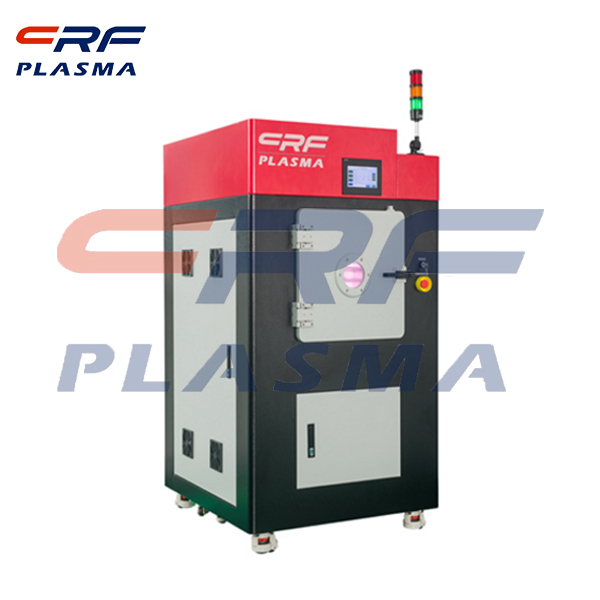
(Summary description)Wafer cleaning is divided into wet cleaning and dry cleaning, plasma cleaning belongs to the latter, mainly used to remove invisible surface contaminants on the wafer surface. In the process of cleaning, first put the chip in the vacuum reaction chamber of plasma cleaning machine, and then pumping air into vacuum state, after reaching a certain degree of vacuum, introducing the reaction gas, the reaction gas ionization plasma formation, and the chip surface, chemical and physical reactions between the volatile substances was siphoned off, make the chip surface clean water. A plasma cleaning machine for cleaning wafers: 1-1: Plasma cleaning of wafers is performed in cleanrooms of class 1000 and above, which requires extremely high particles. Any excessive particles can cause irreparable defects in the wafer. Therefore, the cavity of the plasma cleaning machine must first be aluminum, rather than stainless steel; The sliding part of the bracket where the wafer is placed should be made of materials that are not easy to produce dust and be corroded by plasma. Electrodes and brackets are easy to remove and maintain. 1-2: The electrode spacing, layer number and gas path distribution in the reaction chamber of plasma cleaner have great influence on the uniformity of wafer processing, and these indexes need to be optimized through continuous experiments. 1-3: In the process of plasma cleaning, there will be a certain amount of heat accumulation. It is necessary to keep the temperature of the electrode plate within a certain range, so the electrodes of the plasma cleaning machine are usually cooled by water. 1-4 The relatively high capacity of the multielectrode plasma cleaner allows multiple wafers to be placed on each bracket as needed, making it ideal for the removal of lithographic substrates for 4 "and 6" wafers used for discrete semiconductor devices and power electronic components. Two, plasma cleaning machine for wafer level packaging pretreatment: 2-1: WaferLevelPackage(WLP) is an advanced chip packaging method, that is, after the whole wafer production is completed, directly on the wafer packaging test, and then cut the whole wafer into a single core; The electrical connection uses copper bumps instead of lead bonding, so there is no lead bonding or glue filling process. 2-2: The purpose of wafer level packaging pretreatment is to remove the surface inorganic, reduce the oxide layer, increase the surface roughness of copper and improve the reliability of products. 2-3: Due to the needs of production capacity, there will be significant differences in the design of vacuum reaction chamber, electrode structure, airflow distribution, water cooling device, uniformity and other aspects. 2-4: After the chip is made, the residual photoresist cannot be wet-cleaned, but can only be removed by plasma. But the thickness of photoresist can not be determined, the corresponding process parameters need to be adjusted.
Wafer plasma cleaning machine source manufacturers
(Summary description)Wafer cleaning is divided into wet cleaning and dry cleaning, plasma cleaning belongs to the latter, mainly used to remove invisible surface contaminants on the wafer surface. In the process of cleaning, first put the chip in the vacuum reaction chamber of plasma cleaning machine, and then pumping air into vacuum state, after reaching a certain degree of vacuum, introducing the reaction gas, the reaction gas ionization plasma formation, and the chip surface, chemical and physical reactions between the volatile substances was siphoned off, make the chip surface clean water.
A plasma cleaning machine for cleaning wafers:
1-1:
Plasma cleaning of wafers is performed in cleanrooms of class 1000 and above, which requires extremely high particles. Any excessive particles can cause irreparable defects in the wafer. Therefore, the cavity of the plasma cleaning machine must first be aluminum, rather than stainless steel; The sliding part of the bracket where the wafer is placed should be made of materials that are not easy to produce dust and be corroded by plasma. Electrodes and brackets are easy to remove and maintain.
1-2:
The electrode spacing, layer number and gas path distribution in the reaction chamber of plasma cleaner have great influence on the uniformity of wafer processing, and these indexes need to be optimized through continuous experiments.
1-3:
In the process of plasma cleaning, there will be a certain amount of heat accumulation. It is necessary to keep the temperature of the electrode plate within a certain range, so the electrodes of the plasma cleaning machine are usually cooled by water.
1-4
The relatively high capacity of the multielectrode plasma cleaner allows multiple wafers to be placed on each bracket as needed, making it ideal for the removal of lithographic substrates for 4 "and 6" wafers used for discrete semiconductor devices and power electronic components.
Two, plasma cleaning machine for wafer level packaging pretreatment:
2-1:
WaferLevelPackage(WLP) is an advanced chip packaging method, that is, after the whole wafer production is completed, directly on the wafer packaging test, and then cut the whole wafer into a single core; The electrical connection uses copper bumps instead of lead bonding, so there is no lead bonding or glue filling process.
2-2:
The purpose of wafer level packaging pretreatment is to remove the surface inorganic, reduce the oxide layer, increase the surface roughness of copper and improve the reliability of products.
2-3:
Due to the needs of production capacity, there will be significant differences in the design of vacuum reaction chamber, electrode structure, airflow distribution, water cooling device, uniformity and other aspects.
2-4:
After the chip is made, the residual photoresist cannot be wet-cleaned, but can only be removed by plasma. But the thickness of photoresist can not be determined, the corresponding process parameters need to be adjusted.
- Categories:Technical Support
- Author:plasma cleaning machine-surface treatment equipment-CRF plasma machine-Sing Fung Intelligent Manufacturing
- Origin:
- Time of issue:2021-01-14 09:20
- Views:
Information
Wafer plasma cleaning machine source manufacturers:
Wafer cleaning is divided into wet cleaning and dry cleaning, plasma cleaning belongs to the latter, mainly used to remove invisible surface contaminants on the wafer surface. In the process of cleaning, first put the chip in the vacuum reaction chamber of plasma cleaning machine, and then pumping air into vacuum state, after reaching a certain degree of vacuum, introducing the reaction gas, the reaction gas ionization plasma formation, and the chip surface, chemical and physical reactions between the volatile substances was siphoned off, make the chip surface clean water.
 A plasma cleaning machine for cleaning wafers:
1-1:
Plasma cleaning of wafers is performed in cleanrooms of class 1000 and above, which requires extremely high particles. Any excessive particles can cause irreparable defects in the wafer. Therefore, the cavity of the plasma cleaning machine must first be aluminum, rather than stainless steel; The sliding part of the bracket where the wafer is placed should be made of materials that are not easy to produce dust and be corroded by plasma. Electrodes and brackets are easy to remove and maintain.
1-2:
The electrode spacing, layer number and gas path distribution in the reaction chamber of plasma cleaner have great influence on the uniformity of wafer processing, and these indexes need to be optimized through continuous experiments.
1-3:
In the process of plasma cleaning, there will be a certain amount of heat accumulation. It is necessary to keep the temperature of the electrode plate within a certain range, so the electrodes of the plasma cleaning machine are usually cooled by water.
1-4
The relatively high capacity of the multielectrode plasma cleaner allows multiple wafers to be placed on each bracket as needed, making it ideal for the removal of lithographic substrates for 4 "and 6" wafers used for discrete semiconductor devices and power electronic components.
Two, plasma cleaning machine for wafer level packaging pretreatment:
2-1:
WaferLevelPackage(WLP) is an advanced chip packaging method, that is, after the whole wafer production is completed, directly on the wafer packaging test, and then cut the whole wafer into a single core; The electrical connection uses copper bumps instead of lead bonding, so there is no lead bonding or glue filling process.
2-2:
The purpose of wafer level packaging pretreatment is to remove the surface inorganic, reduce the oxide layer, increase the surface roughness of copper and improve the reliability of products.
2-3:
Due to the needs of production capacity, there will be significant differences in the design of vacuum reaction chamber, electrode structure, airflow distribution, water cooling device, uniformity and other aspects.
2-4:
After the chip is made, the residual photoresist cannot be wet-cleaned, but can only be removed by plasma. But the thickness of photoresist can not be determined, the corresponding process parameters need to be adjusted.
Scan the QR code to read on your phone
Relevant Information


TEL:0755-3367 3020 / 0755-3367 3019

E-mail:sales-sfi@sfi-crf.com

ADD:Mabao Industrial Zone, Huangpu, Baoan District, Shenzhen

