

Welcome to Shenzhen Sing Fung Intelligent Manufacturing Co., Ltd.
E-mail:shaobo@sfi-crf.com


News
Process optimization of plasma cleaning in IC packaging process of plasma industrial cleaning machine
- Categories:Technical Support
- Author:Plasma cleaning machine-CRF plasma plasma equipment-plasma surface treatment machine manufacturer-chengfeng intelligent manufacturing
- Origin:
- Time of issue:2021-07-12
- Views:
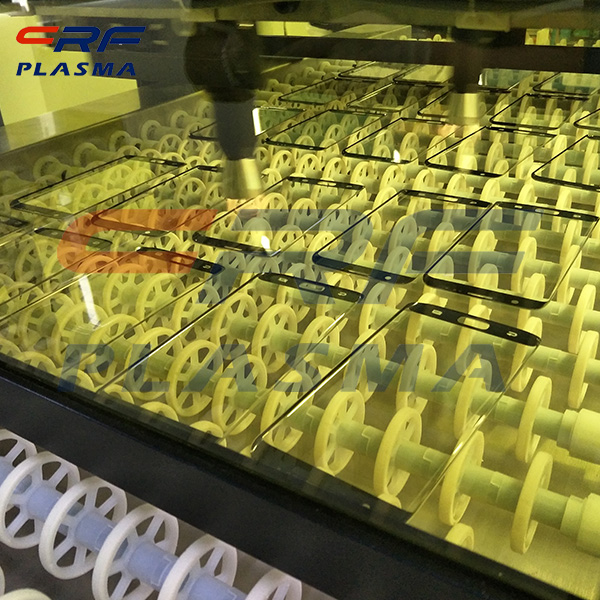
(Summary description)Process optimization of plasma cleaning in IC packaging process of plasma industrial cleaning machine: IC packaging forms vary widely and are constantly evolving, but the production process can be roughly divided into more than a dozen stages, such as wafer cutting, wire bonding in the chip placement rack, and sealing and curing. Only the packaging that meets the requirements can be put into practical application. , Become a terminal product. The quality of packaging will directly affect the cost and performance of electronic products. In IC packaging, about 1/4 device failures are related to contaminants on the surface of the material. How to solve the contaminants such as micro particles and oxide layers in the packaging process , Improving the quality of packaging has become particularly important. The problems in IC packaging mainly include solder delamination, virtual soldering or insufficient wire bonding strength. The culprit of these problems is the pollutants on the lead frame and chip surface, mainly microparticle pollution, oxide layer, organic residues, etc. These existing contaminants make the wire bonding between the chip and the frame substrate incomplete or there is a false solder. Plasma industrial cleaners mainly use active plasma to physically bombard the surface of the material or chemical reactions and other single or dual effects, so as to achieve the removal or modification of contaminants at the molecular level of the surface of the material. Plasma cleaners are effectively used in the IC packaging process to effectively remove organic residues, microparticle contamination, and thin oxide layers on the material surface, improve the surface activity of the workpiece, and avoid bonding delamination or virtual welding. The application of plasma industrial cleaning machines and processes in the field of IC packaging will become more and more extensive, and with their excellent performance, they will become a key production device in the field of IC packaging in the 21st century, and become a means of improving the yield and reliability of products in the mass production process. Important technological measures will be indispensable in the future. The cleaning technology of plasma industrial cleaning machines will also continue to develop and expand the scope of application. As far as the current situation is concerned, it is imperative to promote its process technology to the LED packaging and LCD industries.
Process optimization of plasma cleaning in IC packaging process of plasma industrial cleaning machine
(Summary description)Process optimization of plasma cleaning in IC packaging process of plasma industrial cleaning machine:
IC packaging forms vary widely and are constantly evolving, but the production process can be roughly divided into more than a dozen stages, such as wafer cutting, wire bonding in the chip placement rack, and sealing and curing. Only the packaging that meets the requirements can be put into practical application. , Become a terminal product.
The quality of packaging will directly affect the cost and performance of electronic products. In IC packaging, about 1/4 device failures are related to contaminants on the surface of the material. How to solve the contaminants such as micro particles and oxide layers in the packaging process , Improving the quality of packaging has become particularly important.
The problems in IC packaging mainly include solder delamination, virtual soldering or insufficient wire bonding strength. The culprit of these problems is the pollutants on the lead frame and chip surface, mainly microparticle pollution, oxide layer, organic residues, etc. These existing contaminants make the wire bonding between the chip and the frame substrate incomplete or there is a false solder.
Plasma industrial cleaners mainly use active plasma to physically bombard the surface of the material or chemical reactions and other single or dual effects, so as to achieve the removal or modification of contaminants at the molecular level of the surface of the material. Plasma cleaners are effectively used in the IC packaging process to effectively remove organic residues, microparticle contamination, and thin oxide layers on the material surface, improve the surface activity of the workpiece, and avoid bonding delamination or virtual welding.
The application of plasma industrial cleaning machines and processes in the field of IC packaging will become more and more extensive, and with their excellent performance, they will become a key production device in the field of IC packaging in the 21st century, and become a means of improving the yield and reliability of products in the mass production process. Important technological measures will be indispensable in the future.
The cleaning technology of plasma industrial cleaning machines will also continue to develop and expand the scope of application. As far as the current situation is concerned, it is imperative to promote its process technology to the LED packaging and LCD industries.
- Categories:Technical Support
- Author:Plasma cleaning machine-CRF plasma plasma equipment-plasma surface treatment machine manufacturer-chengfeng intelligent manufacturing
- Origin:
- Time of issue:2021-07-12 21:49
- Views:
Information
Process optimization of plasma cleaning in IC packaging process of plasma industrial cleaning machine:
IC packaging forms vary widely and are constantly evolving, but the production process can be roughly divided into more than a dozen stages, such as wafer cutting, wire bonding in the chip placement rack, and sealing and curing. Only the packaging that meets the requirements can be put into practical application. , Become a terminal product.
The quality of packaging will directly affect the cost and performance of electronic products. In IC packaging, about 1/4 device failures are related to contaminants on the surface of the material. How to solve the contaminants such as micro particles and oxide layers in the packaging process , Improving the quality of packaging has become particularly important.
 The problems in IC packaging mainly include solder delamination, virtual soldering or insufficient wire bonding strength. The culprit of these problems is the pollutants on the lead frame and chip surface, mainly microparticle pollution, oxide layer, organic residues, etc. These existing contaminants make the wire bonding between the chip and the frame substrate incomplete or there is a false solder.
Plasma industrial cleaners mainly use active plasma to physically bombard the surface of the material or chemical reactions and other single or dual effects, so as to achieve the removal or modification of contaminants at the molecular level of the surface of the material. Plasma cleaners are effectively used in the IC packaging process to effectively remove organic residues, microparticle contamination, and thin oxide layers on the material surface, improve the surface activity of the workpiece, and avoid bonding delamination or virtual welding.
The application of plasma industrial cleaning machines and processes in the field of IC packaging will become more and more extensive, and with their excellent performance, they will become a key production device in the field of IC packaging in the 21st century, and become a means of improving the yield and reliability of products in the mass production process. Important technological measures will be indispensable in the future.
The cleaning technology of plasma industrial cleaning machines will also continue to develop and expand the scope of application. As far as the current situation is concerned, it is imperative to promote its process technology to the LED packaging and LCD industries.
Keyword:
Scan the QR code to read on your phone
Relevant Information

After processing the PET film by the plastic plasma processor, observe the processing effect through the contact angle
2021-07-09 08:44

The influence of low-temperature plasma generator on the electrical conductivity and biocompatibility of materials
2021-07-09 08:40

Atmospheric pressure plasma processor for processing metal material welding and surface oil pollution application
2021-07-07 20:35

Plasma treatment of PP fiber composite interface with low temperature plasma treatment instrument
2021-07-06 23:46

Linear automatic plasma cleaning machine improves the bonding force of PI polyimide sputtering copper plating
2021-07-05 22:26

What are the characteristics of the glow discharge potential and light zone distribution of the plasma cleaner
2021-07-04 22:05
Low-temperature plasma processor technology improves the water absorption performance of PET clean cloth
2021-07-03 22:44

The application of plasma cleaning machine effectively increases the product yield to 99.8% and reduces waste
2021-07-02 23:50
Surface modification treatment of inorganic and organic materials by plasma surface cleaning system
2021-07-01 22:23


TEL:0755-3367 3020 / 0755-3367 3019

E-mail:sales-sfi@sfi-crf.com

ADD:Mabao Industrial Zone, Huangpu, Baoan District, Shenzhen

