Welcome to Shenzhen Sing Fung Intelligent Manufacturing Co., Ltd.
E-mail:shaobo@sfi-crf.com
Application of Plasma Cleaning in Packaging Technology for IC IC Manufacturing
- Categories:Technical Support
- Author:plasma cleaning machine-surface treatment equipment-CRF plasma machine-Sing Fung Intelligent Manufacturing
- Origin:
- Time of issue:2021-04-10
- Views:
(Summary description)In the domestic integrated circuit industry chain, the integrated circuit packaging industry is the pillar industry. With the reduction of the size of integrated circuit devices and the improvement of computing speed, packaging technology has become a key technology. The quality and cost of a product are affected by the packaging process. The characteristic size of future IC technology, chip area, the number of transistors contained in the chip and its development trajectory require IC package technology to develop in the direction of miniaturization, low cost, customization, green and environmental protection, and early coordination of package design. Lead frame is a chip carrier, through the bonding wire to achieve the internal circuit of the chip lead terminal and the external lead electrical connection. It is a key structural component that forms the circuit and acts as a bridge with the external leads. Lead frame is an important basic material in the electronic information industry. 1, the basic principle of IC packaging: On the one hand, integrated circuit packaging plays a role in mounting, fixing, sealing, protecting the chip and enhancing the electrothermal performance. On the other hand, it is connected to the pins of the package housing through the contacts on the chip, and these pins are connected to other devices through the wires on the printed circuit board, thus enabling the connection between the internal chip and the external circuit. At the same time, the chip must be isolated from the outside world to prevent the corrosion of the chip circuit by impurities in the air and the degradation of electrical performance. Oxides and particulate contaminants on the chip surface degrade the quality of the product during the packaging of integrated circuits. These contaminants can be effectively removed if plasma cleaning is performed during the packaging process prior to loading, lead bonding, and plastic curing. 2, IC packaging process flow: Only in the IC packaging process of packaging, can it become a terminal product and put into practical application. Integrated circuit packaging process is divided into pre - process, intermediate process and post - process. The packaging technology of integrated circuit has undergone great changes through continuous development. The front-end process can be divided into the following steps: Patch: the protective film and metal frame will be fixed silicon chip cut into silicon chip, and then a single chip; The cutting of a silicon wafer into a single chip for inspection; Chip mounting: place the silver glue or insulating glue at the corresponding position on the lead frame, remove the cut chip from the scribing film and paste it on the fixed position of the lead frame; Bonding: a gold wire is used to connect the lead hole on the chip and the pins on the frame pad, so that the chip is connected to an external circuit; Encapsulation: The circuit that encapsulates a component. Enhance the physical properties of the element to protect the element from external force damage; Post-curing: Curing the plastic packaging material so that it has sufficient hardness and strength to go through the entire packaging process. Pollutants in the process of integrated circuit packaging is an important factor affecting its development, how to solve these problems has been perplexing people, online plasma cleaning technology is a dry cleaning method without any environmental pollution can solve this problem. Plasma cleaning is a process in which the surface of the chip is treated by plasma, so that the contaminants on the sample surface are removed and the surface activity is improved.
Application of Plasma Cleaning in Packaging Technology for IC IC Manufacturing
(Summary description)In the domestic integrated circuit industry chain, the integrated circuit packaging industry is the pillar industry. With the reduction of the size of integrated circuit devices and the improvement of computing speed, packaging technology has become a key technology. The quality and cost of a product are affected by the packaging process. The characteristic size of future IC technology, chip area, the number of transistors contained in the chip and its development trajectory require IC package technology to develop in the direction of miniaturization, low cost, customization, green and environmental protection, and early coordination of package design. Lead frame is a chip carrier, through the bonding wire to achieve the internal circuit of the chip lead terminal and the external lead electrical connection. It is a key structural component that forms the circuit and acts as a bridge with the external leads. Lead frame is an important basic material in the electronic information industry.
1, the basic principle of IC packaging:
On the one hand, integrated circuit packaging plays a role in mounting, fixing, sealing, protecting the chip and enhancing the electrothermal performance. On the other hand, it is connected to the pins of the package housing through the contacts on the chip, and these pins are connected to other devices through the wires on the printed circuit board, thus enabling the connection between the internal chip and the external circuit. At the same time, the chip must be isolated from the outside world to prevent the corrosion of the chip circuit by impurities in the air and the degradation of electrical performance. Oxides and particulate contaminants on the chip surface degrade the quality of the product during the packaging of integrated circuits. These contaminants can be effectively removed if plasma cleaning is performed during the packaging process prior to loading, lead bonding, and plastic curing.
2, IC packaging process flow:
Only in the IC packaging process of packaging, can it become a terminal product and put into practical application. Integrated circuit packaging process is divided into pre - process, intermediate process and post - process. The packaging technology of integrated circuit has undergone great changes through continuous development. The front-end process can be divided into the following steps:
Patch: the protective film and metal frame will be fixed silicon chip cut into silicon chip, and then a single chip;
The cutting of a silicon wafer into a single chip for inspection;
Chip mounting: place the silver glue or insulating glue at the corresponding position on the lead frame, remove the cut chip from the scribing film and paste it on the fixed position of the lead frame;
Bonding: a gold wire is used to connect the lead hole on the chip and the pins on the frame pad, so that the chip is connected to an external circuit;
Encapsulation: The circuit that encapsulates a component. Enhance the physical properties of the element to protect the element from external force damage;
Post-curing: Curing the plastic packaging material so that it has sufficient hardness and strength to go through the entire packaging process.
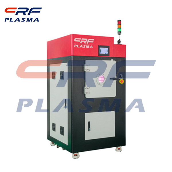
Pollutants in the process of integrated circuit packaging is an important factor affecting its development, how to solve these problems has been perplexing people, online plasma cleaning technology is a dry cleaning method without any environmental pollution can solve this problem. Plasma cleaning is a process in which the surface of the chip is treated by plasma, so that the contaminants on the sample surface are removed and the surface activity is improved.
- Categories:Technical Support
- Author:plasma cleaning machine-surface treatment equipment-CRF plasma machine-Sing Fung Intelligent Manufacturing
- Origin:
- Time of issue:2021-04-10 10:24
- Views:
Application of Plasma Cleaning in Packaging Technology for IC IC Manufacturing:
In the domestic integrated circuit industry chain, the integrated circuit packaging industry is the pillar industry. With the reduction of the size of integrated circuit devices and the improvement of computing speed, packaging technology has become a key technology. The quality and cost of a product are affected by the packaging process. The characteristic size of future IC technology, chip area, the number of transistors contained in the chip and its development trajectory require IC package technology to develop in the direction of miniaturization, low cost, customization, green and environmental protection, and early coordination of package design. Lead frame is a chip carrier, through the bonding wire to achieve the internal circuit of the chip lead terminal and the external lead electrical connection. It is a key structural component that forms the circuit and acts as a bridge with the external leads. Lead frame is an important basic material in the electronic information industry.
1, the basic principle of IC packaging:
On the one hand, integrated circuit packaging plays a role in mounting, fixing, sealing, protecting the chip and enhancing the electrothermal performance. On the other hand, it is connected to the pins of the package housing through the contacts on the chip, and these pins are connected to other devices through the wires on the printed circuit board, thus enabling the connection between the internal chip and the external circuit. At the same time, the chip must be isolated from the outside world to prevent the corrosion of the chip circuit by impurities in the air and the degradation of electrical performance. Oxides and particulate contaminants on the chip surface degrade the quality of the product during the packaging of integrated circuits. These contaminants can be effectively removed if plasma cleaning is performed during the packaging process prior to loading, lead bonding, and plastic curing.
2, IC packaging process flow:
Only in the IC packaging process of packaging, can it become a terminal product and put into practical application. Integrated circuit packaging process is divided into pre - process, intermediate process and post - process. The packaging technology of integrated circuit has undergone great changes through continuous development. The front-end process can be divided into the following steps:
Patch: the protective film and metal frame will be fixed silicon chip cut into silicon chip, and then a single chip;
The cutting of a silicon wafer into a single chip for inspection;
Chip mounting: place the silver glue or insulating glue at the corresponding position on the lead frame, remove the cut chip from the scribing film and paste it on the fixed position of the lead frame;
Bonding: a gold wire is used to connect the lead hole on the chip and the pins on the frame pad, so that the chip is connected to an external circuit;
Encapsulation: The circuit that encapsulates a component. Enhance the physical properties of the element to protect the element from external force damage;
Post-curing: Curing the plastic packaging material so that it has sufficient hardness and strength to go through the entire packaging process.
Pollutants in the process of integrated circuit packaging is an important factor affecting its development, how to solve these problems has been perplexing people, online plasma cleaning technology is a dry cleaning method without any environmental pollution can solve this problem. Plasma cleaning is a process in which the surface of the chip is treated by plasma, so that the contaminants on the sample surface are removed and the surface activity is improved.
Scan the QR code to read on your phone

TEL:0755-3367 3020 / 0755-3367 3019

E-mail:sales-sfi@sfi-crf.com

ADD:Mabao Industrial Zone, Huangpu, Baoan District, Shenzhen


