Welcome to Shenzhen Sing Fung Intelligent Manufacturing Co., Ltd.
E-mail:shaobo@sfi-crf.com
The importance of plasma plasma processor cleaning organic field effect transistor (OFET) materials
- Categories:Company Dynamics
- Author:Plasma cleaning machine-CRF plasma plasma equipment-plasma surface treatment machine manufacturer-chengfeng intelligent manufacturing
- Origin:
- Time of issue:2022-01-05
- Views:
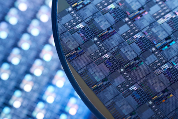
(Summary description)The importance of plasma plasma processor cleaning organic field effect transistor (OFET) materials: Organic Field Effect Transistor (OFETS) is an active device that can change the conductivity of the semiconductor layer by changing the gate voltage, and then manipulate the current flowing through the source and drain. As the basic element in the circuit, the organic field effect transistor has received extensive attention and has been developed rapidly due to its advantages of low power consumption, high impedance, low cost, and large area production. Its components are mainly composed of electrodes, organic semiconductors, heat insulation layers and substrates. These components have a great influence on the performance of OFETs. The electrode, organic semiconductor, insulating layer and substrate are processed by a plasma plasma processor to improve the function of the material. 1. The substrate substrate-plasma plasma treatment machine plasma treatment, remove the substrate surface impurities, improve surface activity The substrate is generally on the bottom layer of the transistor, and the header plays a supporting role. It can be used as the substrate material of OFET: glass, silicon wafer, quartz, polycarbonate (PC), polyethylene naphthalene (PEN), polyimide (PI), polyethylene (PET), etc. Inorganic substrates have the advantages of high melting point and smooth surface, such as glass, silicon wafer, and quartz. Although the surface looks rough, these data show elastic and flexible materials like polyethylene naphthalene (PEN) and polyethylene (PET). The substrate processed by plasma plasma processing machine needs to be processed in the preparation stage to remove impurities on the surface of the substrate and improve surface activity. 2. Electrode treatment-plasma plasma treatment machine plasma treatment In organic field-effect transistors (OFETs), electrodes are another important component. It is generally believed that when the electrical barrier height of the organic semiconductor layer/electrode interface is △E<0.4eV, an ohmic contact can be formed between the electrode and the organic semiconductor layer. For P-type OFETs, the occupied orbital energy level is -4.9 eV to -5.5eV, and a higher work function is required. Commonly used ones are Au (-4.8eV-5.1eV) and ITO (-5.1eV). Ordinary ITO requires an improved work function due to its low work function, so it can be improved with a quasi 13.56MHz frequency VP-R3 plasma processor. 3. Insulation layer treatment-PLASMA plasma retouches the silicone surface to improve the compatibility of materials When the plasma plasma processor is running, the charge is first accumulated and transferred on the contact surface between the semiconductor and the insulating layer. In order to ensure that the gate leakage current between the gate electrode and the organic semiconductor is small, the insulating layer data is required to have a higher resistance. It requires better insulation. At present, the commonly used insulating layer data is first of all inorganic insulating layers, such as oxide layers. During this period, silicon dioxide is the insulating layer generally used in organic field-effect transistors. However, due to the existence of certain defects on the surface of silicon dioxide, in addition to its Number with organic semiconductors
The importance of plasma plasma processor cleaning organic field effect transistor (OFET) materials
(Summary description)The importance of plasma plasma processor cleaning organic field effect transistor (OFET) materials:
Organic Field Effect Transistor (OFETS) is an active device that can change the conductivity of the semiconductor layer by changing the gate voltage, and then manipulate the current flowing through the source and drain. As the basic element in the circuit, the organic field effect transistor has received extensive attention and has been developed rapidly due to its advantages of low power consumption, high impedance, low cost, and large area production. Its components are mainly composed of electrodes, organic semiconductors, heat insulation layers and substrates. These components have a great influence on the performance of OFETs. The electrode, organic semiconductor, insulating layer and substrate are processed by a plasma plasma processor to improve the function of the material.
1. The substrate substrate-plasma plasma treatment machine plasma treatment, remove the substrate surface impurities, improve surface activity
The substrate is generally on the bottom layer of the transistor, and the header plays a supporting role. It can be used as the substrate material of OFET: glass, silicon wafer, quartz, polycarbonate (PC), polyethylene naphthalene (PEN), polyimide (PI), polyethylene (PET), etc. Inorganic substrates have the advantages of high melting point and smooth surface, such as glass, silicon wafer, and quartz. Although the surface looks rough, these data show elastic and flexible materials like polyethylene naphthalene (PEN) and polyethylene (PET). The substrate processed by plasma plasma processing machine needs to be processed in the preparation stage to remove impurities on the surface of the substrate and improve surface activity.
2. Electrode treatment-plasma plasma treatment machine plasma treatment
In organic field-effect transistors (OFETs), electrodes are another important component. It is generally believed that when the electrical barrier height of the organic semiconductor layer/electrode interface is △E<0.4eV, an ohmic contact can be formed between the electrode and the organic semiconductor layer. For P-type OFETs, the occupied orbital energy level is -4.9 eV to -5.5eV, and a higher work function is required. Commonly used ones are Au (-4.8eV-5.1eV) and ITO (-5.1eV). Ordinary ITO requires an improved work function due to its low work function, so it can be improved with a quasi 13.56MHz frequency VP-R3 plasma processor.
3. Insulation layer treatment-PLASMA plasma retouches the silicone surface to improve the compatibility of materials
When the plasma plasma processor is running, the charge is first accumulated and transferred on the contact surface between the semiconductor and the insulating layer. In order to ensure that the gate leakage current between the gate electrode and the organic semiconductor is small, the insulating layer data is required to have a higher resistance. It requires better insulation. At present, the commonly used insulating layer data is first of all inorganic insulating layers, such as oxide layers. During this period, silicon dioxide is the insulating layer generally used in organic field-effect transistors. However, due to the existence of certain defects on the surface of silicon dioxide, in addition to its Number with organic semiconductors
- Categories:Company Dynamics
- Author:Plasma cleaning machine-CRF plasma plasma equipment-plasma surface treatment machine manufacturer-chengfeng intelligent manufacturing
- Origin:
- Time of issue:2022-01-05 17:19
- Views:
The importance of plasma plasma processor cleaning organic field effect transistor (OFET) materials:
Organic Field Effect Transistor (OFETS) is an active device that can change the conductivity of the semiconductor layer by changing the gate voltage, and then manipulate the current flowing through the source and drain. As the basic element in the circuit, the organic field effect transistor has received extensive attention and has been developed rapidly due to its advantages of low power consumption, high impedance, low cost, and large area production. Its components are mainly composed of electrodes, organic semiconductors, heat insulation layers and substrates. These components have a great influence on the performance of OFETs. The electrode, organic semiconductor, insulating layer and substrate are processed by a plasma plasma processor to improve the function of the material.
1. The substrate substrate-plasma plasma treatment machine plasma treatment, remove the substrate surface impurities, improve surface activity
The substrate is generally on the bottom layer of the transistor, and the header plays a supporting role. It can be used as the substrate material of OFET: glass, silicon wafer, quartz, polycarbonate (PC), polyethylene naphthalene (PEN), polyimide (PI), polyethylene (PET), etc. Inorganic substrates have the advantages of high melting point and smooth surface, such as glass, silicon wafer, and quartz. Although the surface looks rough, these data show elastic and flexible materials like polyethylene naphthalene (PEN) and polyethylene (PET). The substrate processed by plasma plasma processing machine needs to be processed in the preparation stage to remove impurities on the surface of the substrate and improve surface activity.
 2. Electrode treatment-plasma plasma treatment machine plasma treatment
In organic field-effect transistors (OFETs), electrodes are another important component. It is generally believed that when the electrical barrier height of the organic semiconductor layer/electrode interface is △E<0.4eV, an ohmic contact can be formed between the electrode and the organic semiconductor layer. For P-type OFETs, the occupied orbital energy level is -4.9 eV to -5.5eV, and a higher work function is required. Commonly used ones are Au (-4.8eV-5.1eV) and ITO (-5.1eV). Ordinary ITO requires an improved work function due to its low work function, so it can be improved with a quasi 13.56MHz frequency VP-R3 plasma processor.
3. Insulation layer treatment-PLASMA plasma retouches the silicone surface to improve the compatibility of materials
When the plasma plasma processor is running, the charge is first accumulated and transferred on the contact surface between the semiconductor and the insulating layer. In order to ensure that the gate leakage current between the gate electrode and the organic semiconductor is small, the insulating layer data is required to have a higher resistance. It requires better insulation. At present, the commonly used insulating layer data is first of all inorganic insulating layers, such as oxide layers. During this period, silicon dioxide is the insulating layer generally used in organic field-effect transistors. However, due to the existence of certain defects on the surface of silicon dioxide, in addition to its Number with organic semiconductors
Scan the QR code to read on your phone

TEL:0755-3367 3020 / 0755-3367 3019

E-mail:sales-sfi@sfi-crf.com

ADD:Mabao Industrial Zone, Huangpu, Baoan District, Shenzhen


