

Welcome to Shenzhen Sing Fung Intelligent Manufacturing Co., Ltd.
E-mail:shaobo@sfi-crf.com


News
Removal of pollutant molecules in the production process of microelectronics packaging of plasma processing equipment
- Categories:Company Dynamics
- Author:Plasma cleaning machine-CRF plasma plasma equipment-plasma surface treatment machine manufacturer-chengfeng intelligent manufacturing
- Origin:
- Time of issue:2022-01-02
- Views:
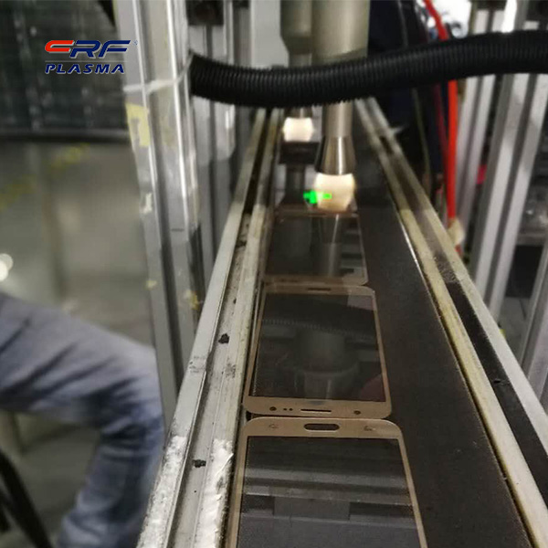
(Summary description)Removal of pollutant molecules in the production process of microelectronics packaging of plasma processing equipment: In the microelectronics industry, cleaning is a broad concept that includes all processes related to the removal of pollutants. Generally, it refers to effectively removing residual dust, metal ions, and organic impurities on the surface of the data without destroying the surface and electrical characteristics of the data. At present, the widely used physical and chemical cleaning methods can be roughly divided into two types: wet cleaning and dry cleaning of plasma treatment equipment. At present, wet cleaning still occupies the leading position in the cleaning process of microelectronics. However, from the perspective of environmental impact, consumption of original materials and future development, dry cleaning is significantly better than wet cleaning. Dry cleaning has developed rapidly and has obvious advantages. Plasma processing equipment cleaning has gradually begun to be widely used in semiconductor manufacturing, microelectronic packaging, precision machinery and other industries. The major feature of plasma processing equipment technology is that regardless of the type of substrate to be processed, it can process metals, semiconductors, oxides and most polymer materials, such as polypropylene, polyester, polyimide, and polychloride. Ethane, epoxy and even polytetrafluoroethylene, etc., can be used for comprehensive, partial and messy structure cleaning. Plasma treatment equipment cleaning also has the following characteristics: simple numerical control technology, high degree of automation; high precision of the operating device; no damage layer on the surface, material quality is guaranteed; vacuum from the inside out, does not pollute the environment, and ensures that the surface is cleaned Not subject to secondary pollution. In the production process of microelectronics packaging, due to fingerprints, flux, various cross-contamination, natural oxidation, etc., various dirts will be formed on the surface of equipment and materials, including organic matter, epoxy resin, photoresist, solder, metal salt, etc. This will have a significant impact on the quality of related processes in the packaging production process. Plasma cleaning with plasma processing equipment can easily eliminate the pollutant molecules generated during the production process, ensure the close contact between the surface atoms of the workpiece and the plasma atoms, and then effectively improve the wire connection strength, improve the quality of wafer bonding, and reduce package leakage. Gas rate, improve component performance, increase yield and reliability. Before the aluminum wire connection, a certain domestic unit used the plasma cleaning method to increase the connection yield by 30% and the consistency of the connection strength.
Removal of pollutant molecules in the production process of microelectronics packaging of plasma processing equipment
(Summary description)Removal of pollutant molecules in the production process of microelectronics packaging of plasma processing equipment:
In the microelectronics industry, cleaning is a broad concept that includes all processes related to the removal of pollutants. Generally, it refers to effectively removing residual dust, metal ions, and organic impurities on the surface of the data without destroying the surface and electrical characteristics of the data. At present, the widely used physical and chemical cleaning methods can be roughly divided into two types: wet cleaning and dry cleaning of plasma treatment equipment.
At present, wet cleaning still occupies the leading position in the cleaning process of microelectronics. However, from the perspective of environmental impact, consumption of original materials and future development, dry cleaning is significantly better than wet cleaning. Dry cleaning has developed rapidly and has obvious advantages. Plasma processing equipment cleaning has gradually begun to be widely used in semiconductor manufacturing, microelectronic packaging, precision machinery and other industries.
The major feature of plasma processing equipment technology is that regardless of the type of substrate to be processed, it can process metals, semiconductors, oxides and most polymer materials, such as polypropylene, polyester, polyimide, and polychloride. Ethane, epoxy and even polytetrafluoroethylene, etc., can be used for comprehensive, partial and messy structure cleaning. Plasma treatment equipment cleaning also has the following characteristics: simple numerical control technology, high degree of automation; high precision of the operating device; no damage layer on the surface, material quality is guaranteed; vacuum from the inside out, does not pollute the environment, and ensures that the surface is cleaned Not subject to secondary pollution.
In the production process of microelectronics packaging, due to fingerprints, flux, various cross-contamination, natural oxidation, etc., various dirts will be formed on the surface of equipment and materials, including organic matter, epoxy resin, photoresist, solder, metal salt, etc. This will have a significant impact on the quality of related processes in the packaging production process. Plasma cleaning with plasma processing equipment can easily eliminate the pollutant molecules generated during the production process, ensure the close contact between the surface atoms of the workpiece and the plasma atoms, and then effectively improve the wire connection strength, improve the quality of wafer bonding, and reduce package leakage. Gas rate, improve component performance, increase yield and reliability. Before the aluminum wire connection, a certain domestic unit used the plasma cleaning method to increase the connection yield by 30% and the consistency of the connection strength.
- Categories:Company Dynamics
- Author:Plasma cleaning machine-CRF plasma plasma equipment-plasma surface treatment machine manufacturer-chengfeng intelligent manufacturing
- Origin:
- Time of issue:2022-01-02 15:27
- Views:
Information
Removal of pollutant molecules in the production process of microelectronics packaging of plasma processing equipment:
In the microelectronics industry, cleaning is a broad concept that includes all processes related to the removal of pollutants. Generally, it refers to effectively removing residual dust, metal ions, and organic impurities on the surface of the data without destroying the surface and electrical characteristics of the data. At present, the widely used physical and chemical cleaning methods can be roughly divided into two types: wet cleaning and dry cleaning of plasma treatment equipment.
 At present, wet cleaning still occupies the leading position in the cleaning process of microelectronics. However, from the perspective of environmental impact, consumption of original materials and future development, dry cleaning is significantly better than wet cleaning. Dry cleaning has developed rapidly and has obvious advantages. Plasma processing equipment cleaning has gradually begun to be widely used in semiconductor manufacturing, microelectronic packaging, precision machinery and other industries.
The major feature of plasma processing equipment technology is that regardless of the type of substrate to be processed, it can process metals, semiconductors, oxides and most polymer materials, such as polypropylene, polyester, polyimide, and polychloride. Ethane, epoxy and even polytetrafluoroethylene, etc., can be used for comprehensive, partial and messy structure cleaning. Plasma treatment equipment cleaning also has the following characteristics: simple numerical control technology, high degree of automation; high precision of the operating device; no damage layer on the surface, material quality is guaranteed; vacuum from the inside out, does not pollute the environment, and ensures that the surface is cleaned Not subject to secondary pollution.
In the production process of microelectronics packaging, due to fingerprints, flux, various cross-contamination, natural oxidation, etc., various dirts will be formed on the surface of equipment and materials, including organic matter, epoxy resin, photoresist, solder, metal salt, etc. This will have a significant impact on the quality of related processes in the packaging production process. Plasma cleaning with plasma processing equipment can easily eliminate the pollutant molecules generated during the production process, ensure the close contact between the surface atoms of the workpiece and the plasma atoms, and then effectively improve the wire connection strength, improve the quality of wafer bonding, and reduce package leakage. Gas rate, improve component performance, increase yield and reliability. Before the aluminum wire connection, a certain domestic unit used the plasma cleaning method to increase the connection yield by 30% and the consistency of the connection strength.
Scan the QR code to read on your phone
Relevant Information


The low-temperature plasma has enough energy to break the chemical bonds in the biomass feedstock
2021-12-31 15:24

Plasma glass cleaning machines are widely used in manufacturing industries such as mobile phone coating and new materials
2021-12-30 15:22

The plasma generator power supply chooses different process gas classification and action mechanism
2021-12-29 19:55

The bonding and other processes can only be implemented after the metal plastic activation treatment of the oxygen plasma cleaner
2021-12-28 19:54

Plasma surface activation treatment method of plasma etching process to remove static electricity
2021-12-27 16:53

The surface of the glass plasma cleaner is cleaned and coated to improve the bonding strength
2021-12-26 16:52

Plasma cleaning machine cleans polymer plays a role in surface reorganization, cleaning, modification, etc.
2021-12-25 17:03

5 major surface treatment technologies, take stock of those surface treatment processes that you don’t know
2021-12-24 17:01


TEL:0755-3367 3020 / 0755-3367 3019

E-mail:sales-sfi@sfi-crf.com

ADD:Mabao Industrial Zone, Huangpu, Baoan District, Shenzhen

