

Welcome to Shenzhen Sing Fung Intelligent Manufacturing Co., Ltd.
E-mail:shaobo@sfi-crf.com


News
Plasma etching cleaning machine ICP etching technology is widely used in SiC etching applications
- Categories:Technical Support
- Author:Plasma cleaning machine-CRF plasma plasma equipment-plasma surface treatment machine manufacturer-chengfeng intelligent manufacturing
- Origin:
- Time of issue:2022-01-04
- Views:
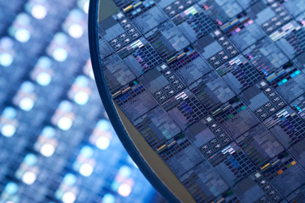
(Summary description)Plasma etching cleaning machine ICP etching technology is widely used in SiC etching applications: Reaction-bonded silicon carbide (RB-SiC), as a new type of ceramic material, has the characteristics of high strength, specific stiffness, large thermal conductivity and small expansion coefficient. With the rapid development of optical technology, optical systems are moving towards large-diameter, low-caliber The development of loss and lightweight requires optical components with high resolution, wide field of view, and high-quality surface topography RB-SiC material has been widely used due to its superior performance, which puts forward higher requirements on the optical quality of the surface of the material. There are many methods for processing SiC, mainly including electrochemical corrosion, mechanical processing, ultrasonic processing, laser etching and plasma dry etching. The plasma dry etching technology of plasma etching cleaner mainly includes reactive ion etching (RIE), electron cyclotron resonance (ECR) and inductively coupled plasma (ICP). ICP etching equipment has the advantages of selectivity and anisotropic structure, simple operation, convenient control, etc. Therefore, ICP etching technology is widely used in SiC etching applications. Plasma Etching Cleaner ICP etching technology is mainly used in the processing and production of SiC semiconductor devices and micro-electromechanical systems (MEMS) devices, etching the surface quality, and improving the performance and quality of SiC microwave power devices. The complete etching process of ICP etching technology can be divided into three steps: ① adsorption of etched substances; ② formation of volatiles; ③ desorption. It includes two processes, chemical and physical: in the chemical process, the etching gas generates active radicals, metastable particles and electrons through inductive coupling through glow discharge, and the neutral particles diffuse to the surface of the substrate and are etched. The atoms on the material surface chemically react to produce volatile substances, and these by-products are drawn out of the chamber by the vacuum system to achieve gas chemical etching. In addition, the physical process is through ion bombardment of the etched substrate surface. Unlike sputter etching, the physical bombardment here is mainly to destroy chemical bonds and lattice sequences, accelerate the desorption of reactants, and promote the chemical reaction process. Carry out and remove non-volatile products on the surface. In the etching process of the plasma etching cleaner ICP, the substrate bias voltage provides energy for the plasma, enabling active particles to act on the surface of the substrate. The power determines the kinetic energy of the plasma. These high-energy active particles are in the etching process. , Plays an important role. Compared with the etching before and after the etching, the surface quality has declined. Analyze the reason. The active particles generated by the ICP etching glow discharge diffuse to the surface of the substrate and the chemical reaction will generate some non-volatile products, which is too late for desorption and deposition. To the surface of the substrate. In addition, some ions have physical bombardment on the substrate, destroying the surface lattice array, causing holes and pits on the surface of the substrate, resulting in a decrease in the surface quality of the material. At the same time, the structure of the original substrate is not uniform due to the presence of two-phase components of silicon and silicon carbide. The non-uniformity of the two-phase boundary, holes and pits on the surface of the material after plasma etching by the plasma etching cleaner will cause the scattering of light on the surface of the material, and the holes will also increase the absorption of light by the material. The surface reflectivity decreases and the surface roughness increases.
Plasma etching cleaning machine ICP etching technology is widely used in SiC etching applications
(Summary description)Plasma etching cleaning machine ICP etching technology is widely used in SiC etching applications:
Reaction-bonded silicon carbide (RB-SiC), as a new type of ceramic material, has the characteristics of high strength, specific stiffness, large thermal conductivity and small expansion coefficient. With the rapid development of optical technology, optical systems are moving towards large-diameter, low-caliber The development of loss and lightweight requires optical components with high resolution, wide field of view, and high-quality surface topography
RB-SiC material has been widely used due to its superior performance, which puts forward higher requirements on the optical quality of the surface of the material. There are many methods for processing SiC, mainly including electrochemical corrosion, mechanical processing, ultrasonic processing, laser etching and plasma dry etching. The plasma dry etching technology of plasma etching cleaner mainly includes reactive ion etching (RIE), electron cyclotron resonance (ECR) and inductively coupled plasma (ICP). ICP etching equipment has the advantages of selectivity and anisotropic structure, simple operation, convenient control, etc. Therefore, ICP etching technology is widely used in SiC etching applications.
Plasma Etching Cleaner ICP etching technology is mainly used in the processing and production of SiC semiconductor devices and micro-electromechanical systems (MEMS) devices, etching the surface quality, and improving the performance and quality of SiC microwave power devices. The complete etching process of ICP etching technology can be divided into three steps: ① adsorption of etched substances; ② formation of volatiles; ③ desorption. It includes two processes, chemical and physical: in the chemical process, the etching gas generates active radicals, metastable particles and electrons through inductive coupling through glow discharge, and the neutral particles diffuse to the surface of the substrate and are etched. The atoms on the material surface chemically react to produce volatile substances, and these by-products are drawn out of the chamber by the vacuum system to achieve gas chemical etching.
In addition, the physical process is through ion bombardment of the etched substrate surface. Unlike sputter etching, the physical bombardment here is mainly to destroy chemical bonds and lattice sequences, accelerate the desorption of reactants, and promote the chemical reaction process. Carry out and remove non-volatile products on the surface. In the etching process of the plasma etching cleaner ICP, the substrate bias voltage provides energy for the plasma, enabling active particles to act on the surface of the substrate. The power determines the kinetic energy of the plasma. These high-energy active particles are in the etching process. , Plays an important role.
Compared with the etching before and after the etching, the surface quality has declined. Analyze the reason. The active particles generated by the ICP etching glow discharge diffuse to the surface of the substrate and the chemical reaction will generate some non-volatile products, which is too late for desorption and deposition. To the surface of the substrate. In addition, some ions have physical bombardment on the substrate, destroying the surface lattice array, causing holes and pits on the surface of the substrate, resulting in a decrease in the surface quality of the material. At the same time, the structure of the original substrate is not uniform due to the presence of two-phase components of silicon and silicon carbide. The non-uniformity of the two-phase boundary, holes and pits on the surface of the material after plasma etching by the plasma etching cleaner will cause the scattering of light on the surface of the material, and the holes will also increase the absorption of light by the material. The surface reflectivity decreases and the surface roughness increases.
- Categories:Technical Support
- Author:Plasma cleaning machine-CRF plasma plasma equipment-plasma surface treatment machine manufacturer-chengfeng intelligent manufacturing
- Origin:
- Time of issue:2022-01-04 16:56
- Views:
Information
Plasma etching cleaning machine ICP etching technology is widely used in SiC etching applications:
Reaction-bonded silicon carbide (RB-SiC), as a new type of ceramic material, has the characteristics of high strength, specific stiffness, large thermal conductivity and small expansion coefficient. With the rapid development of optical technology, optical systems are moving towards large-diameter, low-caliber The development of loss and lightweight requires optical components with high resolution, wide field of view, and high-quality surface topography
RB-SiC material has been widely used due to its superior performance, which puts forward higher requirements on the optical quality of the surface of the material. There are many methods for processing SiC, mainly including electrochemical corrosion, mechanical processing, ultrasonic processing, laser etching and plasma dry etching. The plasma dry etching technology of plasma etching cleaner mainly includes reactive ion etching (RIE), electron cyclotron resonance (ECR) and inductively coupled plasma (ICP). ICP etching equipment has the advantages of selectivity and anisotropic structure, simple operation, convenient control, etc. Therefore, ICP etching technology is widely used in SiC etching applications.
 Plasma Etching Cleaner ICP etching technology is mainly used in the processing and production of SiC semiconductor devices and micro-electromechanical systems (MEMS) devices, etching the surface quality, and improving the performance and quality of SiC microwave power devices. The complete etching process of ICP etching technology can be divided into three steps: ① adsorption of etched substances; ② formation of volatiles; ③ desorption. It includes two processes, chemical and physical: in the chemical process, the etching gas generates active radicals, metastable particles and electrons through inductive coupling through glow discharge, and the neutral particles diffuse to the surface of the substrate and are etched. The atoms on the material surface chemically react to produce volatile substances, and these by-products are drawn out of the chamber by the vacuum system to achieve gas chemical etching.
In addition, the physical process is through ion bombardment of the etched substrate surface. Unlike sputter etching, the physical bombardment here is mainly to destroy chemical bonds and lattice sequences, accelerate the desorption of reactants, and promote the chemical reaction process. Carry out and remove non-volatile products on the surface. In the etching process of the plasma etching cleaner ICP, the substrate bias voltage provides energy for the plasma, enabling active particles to act on the surface of the substrate. The power determines the kinetic energy of the plasma. These high-energy active particles are in the etching process. , Plays an important role.
Compared with the etching before and after the etching, the surface quality has declined. Analyze the reason. The active particles generated by the ICP etching glow discharge diffuse to the surface of the substrate and the chemical reaction will generate some non-volatile products, which is too late for desorption and deposition. To the surface of the substrate. In addition, some ions have physical bombardment on the substrate, destroying the surface lattice array, causing holes and pits on the surface of the substrate, resulting in a decrease in the surface quality of the material. At the same time, the structure of the original substrate is not uniform due to the presence of two-phase components of silicon and silicon carbide. The non-uniformity of the two-phase boundary, holes and pits on the surface of the material after plasma etching by the plasma etching cleaner will cause the scattering of light on the surface of the material, and the holes will also increase the absorption of light by the material. The surface reflectivity decreases and the surface roughness increases.
Scan the QR code to read on your phone
Relevant Information

Study on the experimental nucleation of plasma chemical vapor deposition diamond film
2022-01-03 16:55

Removal of pollutant molecules in the production process of microelectronics packaging of plasma processing equipment
2022-01-02 15:27


The low-temperature plasma has enough energy to break the chemical bonds in the biomass feedstock
2021-12-31 15:24
Plasma glass cleaning machines are widely used in manufacturing industries such as mobile phone coating and new materials
2021-12-30 15:22

The plasma generator power supply chooses different process gas classification and action mechanism
2021-12-29 19:55

The bonding and other processes can only be implemented after the metal plastic activation treatment of the oxygen plasma cleaner
2021-12-28 19:54

Plasma surface activation treatment method of plasma etching process to remove static electricity
2021-12-27 16:53

The surface of the glass plasma cleaner is cleaned and coated to improve the bonding strength
2021-12-26 16:52

Plasma cleaning machine cleans polymer plays a role in surface reorganization, cleaning, modification, etc.
2021-12-25 17:03


TEL:0755-3367 3020 / 0755-3367 3019

E-mail:sales-sfi@sfi-crf.com

ADD:Mabao Industrial Zone, Huangpu, Baoan District, Shenzhen

