

Welcome to Shenzhen Sing Fung Intelligent Manufacturing Co., Ltd.
E-mail:shaobo@sfi-crf.com


News
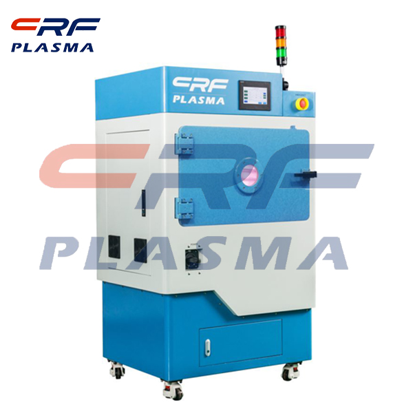
Application of semiconductor plasma cleaning machine in wafer cleaning
- Categories:Company Dynamics
- Author:plasma cleaning machine-surface treatment equipment-CRF plasma machine-Sing Fung Intelligent Manufacturing
- Origin:
- Time of issue:2020-10-13
- Views:
(Summary description)With the continuous development of semiconductor technology, the requirement of process technology is higher and higher, especially the surface quality of semiconductor chip. The main reason is that the particles and metal impurities on the surface of the chip will seriously affect the quality and yield of the device. In the current IC production, there is still more than 50% material loss due to the pollution of the wafer surface. In semiconductor manufacturing, almost every process needs cleaning, and the quality of wafer cleaning has a serious impact on device performance. It is precisely because wafer cleaning is the most important and frequent step in semiconductor manufacturing process, and its process quality will directly affect the yield, performance and reliability of the device, so companies and research institutions at home and abroad have been constantly studying the cleaning process. Plasma cleaning, as an advanced dry cleaning technology, has the characteristics of environmental protection. With the rapid development of microelectronics industry, plasma cleaning machine has been used more and more in semiconductor industry. Plasma cleaning has the advantages of simple process, easy operation, no waste treatment and environmental pollution. Plasma cleaning is commonly used in photoresist removal. A small amount of oxygen is introduced into the plasma reaction system. Under the action of a strong electric field, oxygen produces plasma, which rapidly oxidizes the photoresist into volatile gas and is pumped away. This cleaning technology has the advantages of easy operation, high efficiency, clean surface, no scratch and so on, which is helpful to guarantee the product quality. And do not use acid, alkali, organic solvents, more and more attention by people. The following is a brief introduction to the impurities and classification of semiconductors: Semiconductor manufacturing requires the participation of some organic and inorganic materials. In addition, because the process is always carried out by people in the purification room, the semiconductor chip will inevitably be contaminated with various impurities. According to the sources and properties of pollutants, they can be roughly classified into four categories: particles, organic matter, metal ions and oxides. 1.1 particles: Particles are mainly polymers, photoresist and etching impurities. This contaminant is usually adsorbed on the wafer surface and affects the geometric pattern formation and electrical parameters of the photolithography process. The removal method of this kind of pollutant is mainly to clean the particles through physical or chemical methods, gradually reduce the contact area between particles and the surface of the wafer, and finally remove. 1.2 Organic matters: Organic impurities come from a wide range of sources, such as human skin oils, bacteria, oil, vacuum oils, photoresist, cleaning solvents, etc. These contaminants usually form an organic film on the surface of the wafer to prevent the cleaning solution from reaching the wafer surface, resulting in incomplete surface cleaning and leaving contaminants such as metal impurities on the surface intact. Removal of such contaminants is usually done in the first step of the cleaning process, using mainly sulfuric acid and hydrogen peroxide. 1.3 metals: Common metal impurities in semiconductor technology include iron, copper, aluminum, chromium, tungsten, titanium, sodium, potassium, lithium and so on. The sources of these impurities include various containers, pipes, chemical reagents, and metal contamination in semiconductor wafer processing. Chemical methods are often used to remove such impurities. Cleaning fluids prepared with various reagents and chemicals react with metal ions to form metal ion complexes, which are separated from the wafer surface. 1.4 Oxide: A natural oxide layer forms on the surface of a semiconductor chip exposed to oxygen and water. Not only does this oxide film block many of the steps in semiconductor manufacturing, but it also contains metal impurities that, under certain conditions, can transfer to the chip and form electrical defects. The removal of this oxide film is usually accomplished by immersion in dilute hydrofluoric acid.
Application of semiconductor plasma cleaning machine in wafer cleaning
(Summary description)With the continuous development of semiconductor technology, the requirement of process technology is higher and higher, especially the surface quality of semiconductor chip. The main reason is that the particles and metal impurities on the surface of the chip will seriously affect the quality and yield of the device. In the current IC production, there is still more than 50% material loss due to the pollution of the wafer surface.
In semiconductor manufacturing, almost every process needs cleaning, and the quality of wafer cleaning has a serious impact on device performance. It is precisely because wafer cleaning is the most important and frequent step in semiconductor manufacturing process, and its process quality will directly affect the yield, performance and reliability of the device, so companies and research institutions at home and abroad have been constantly studying the cleaning process. Plasma cleaning, as an advanced dry cleaning technology, has the characteristics of environmental protection. With the rapid development of microelectronics industry, plasma cleaning machine has been used more and more in semiconductor industry.
Plasma cleaning has the advantages of simple process, easy operation, no waste treatment and environmental pollution. Plasma cleaning is commonly used in photoresist removal. A small amount of oxygen is introduced into the plasma reaction system. Under the action of a strong electric field, oxygen produces plasma, which rapidly oxidizes the photoresist into volatile gas and is pumped away. This cleaning technology has the advantages of easy operation, high efficiency, clean surface, no scratch and so on, which is helpful to guarantee the product quality. And do not use acid, alkali, organic solvents, more and more attention by people.
The following is a brief introduction to the impurities and classification of semiconductors:
Semiconductor manufacturing requires the participation of some organic and inorganic materials. In addition, because the process is always carried out by people in the purification room, the semiconductor chip will inevitably be contaminated with various impurities. According to the sources and properties of pollutants, they can be roughly classified into four categories: particles, organic matter, metal ions and oxides.
1.1 particles:
Particles are mainly polymers, photoresist and etching impurities. This contaminant is usually adsorbed on the wafer surface and affects the geometric pattern formation and electrical parameters of the photolithography process. The removal method of this kind of pollutant is mainly to clean the particles through physical or chemical methods, gradually reduce the contact area between particles and the surface of the wafer, and finally remove.
1.2 Organic matters:
Organic impurities come from a wide range of sources, such as human skin oils, bacteria, oil, vacuum oils, photoresist, cleaning solvents, etc. These contaminants usually form an organic film on the surface of the wafer to prevent the cleaning solution from reaching the wafer surface, resulting in incomplete surface cleaning and leaving contaminants such as metal impurities on the surface intact. Removal of such contaminants is usually done in the first step of the cleaning process, using mainly sulfuric acid and hydrogen peroxide.
1.3 metals:
Common metal impurities in semiconductor technology include iron, copper, aluminum, chromium, tungsten, titanium, sodium, potassium, lithium and so on. The sources of these impurities include various containers, pipes, chemical reagents, and metal contamination in semiconductor wafer processing. Chemical methods are often used to remove such impurities. Cleaning fluids prepared with various reagents and chemicals react with metal ions to form metal ion complexes, which are separated from the wafer surface.
1.4 Oxide:
A natural oxide layer forms on the surface of a semiconductor chip exposed to oxygen and water. Not only does this oxide film block many of the steps in semiconductor manufacturing, but it also contains metal impurities that, under certain conditions, can transfer to the chip and form electrical defects. The removal of this oxide film is usually accomplished by immersion in dilute hydrofluoric acid.
- Categories:Company Dynamics
- Author:plasma cleaning machine-surface treatment equipment-CRF plasma machine-Sing Fung Intelligent Manufacturing
- Origin:
- Time of issue:2020-10-13 09:11
- Views:
Information
Application of semiconductor plasma cleaning machine in wafer cleaning:
With the continuous development of semiconductor technology, the requirement of process technology is higher and higher, especially the surface quality of semiconductor chip. The main reason is that the particles and metal impurities on the surface of the chip will seriously affect the quality and yield of the device. In the current IC production, there is still more than 50% material loss due to the pollution of the wafer surface.
In semiconductor manufacturing, almost every process needs cleaning, and the quality of wafer cleaning has a serious impact on device performance. It is precisely because wafer cleaning is the most important and frequent step in semiconductor manufacturing process, and its process quality will directly affect the yield, performance and reliability of the device, so companies and research institutions at home and abroad have been constantly studying the cleaning process. Plasma cleaning, as an advanced dry cleaning technology, has the characteristics of environmental protection. With the rapid development of microelectronics industry, plasma cleaning machine has been used more and more in semiconductor industry.
Plasma cleaning has the advantages of simple process, easy operation, no waste treatment and environmental pollution. Plasma cleaning is commonly used in photoresist removal. A small amount of oxygen is introduced into the plasma reaction system. Under the action of a strong electric field, oxygen produces plasma, which rapidly oxidizes the photoresist into volatile gas and is pumped away. This cleaning technology has the advantages of easy operation, high efficiency, clean surface, no scratch and so on, which is helpful to guarantee the product quality. And do not use acid, alkali, organic solvents, more and more attention by people.
The following is a brief introduction to the impurities and classification of semiconductors:
Semiconductor manufacturing requires the participation of some organic and inorganic materials. In addition, because the process is always carried out by people in the purification room, the semiconductor chip will inevitably be contaminated with various impurities. According to the sources and properties of pollutants, they can be roughly classified into four categories: particles, organic matter, metal ions and oxides.
1.1 particles:
Particles are mainly polymers, photoresist and etching impurities. This contaminant is usually adsorbed on the wafer surface and affects the geometric pattern formation and electrical parameters of the photolithography process. The removal method of this kind of pollutant is mainly to clean the particles through physical or chemical methods, gradually reduce the contact area between particles and the surface of the wafer, and finally remove.
1.2 Organic matters:
Organic impurities come from a wide range of sources, such as human skin oils, bacteria, oil, vacuum oils, photoresist, cleaning solvents, etc. These contaminants usually form an organic film on the surface of the wafer to prevent the cleaning solution from reaching the wafer surface, resulting in incomplete surface cleaning and leaving contaminants such as metal impurities on the surface intact. Removal of such contaminants is usually done in the first step of the cleaning process, using mainly sulfuric acid and hydrogen peroxide.
1.3 metals:
Common metal impurities in semiconductor technology include iron, copper, aluminum, chromium, tungsten, titanium, sodium, potassium, lithium and so on. The sources of these impurities include various containers, pipes, chemical reagents, and metal contamination in semiconductor wafer processing. Chemical methods are often used to remove such impurities. Cleaning fluids prepared with various reagents and chemicals react with metal ions to form metal ion complexes, which are separated from the wafer surface.
1.4 Oxide:
A natural oxide layer forms on the surface of a semiconductor chip exposed to oxygen and water. Not only does this oxide film block many of the steps in semiconductor manufacturing, but it also contains metal impurities that, under certain conditions, can transfer to the chip and form electrical defects. The removal of this oxide film is usually accomplished by immersion in dilute hydrofluoric acid.
Scan the QR code to read on your phone
Relevant Information


Plasma surface treatment can improve the hydrophilic bonding ability of steel /EPDM surface
2020-10-07 09:42


TEL:0755-3367 3020 / 0755-3367 3019

E-mail:sales-sfi@sfi-crf.com

ADD:Mabao Industrial Zone, Huangpu, Baoan District, Shenzhen

