Welcome to Shenzhen Sing Fung Intelligent Manufacturing Co., Ltd.
E-mail:shaobo@sfi-crf.com
Empirical analysis of graphene etching principle of plasma surface processor manufacturers
- Categories:Company Dynamics
- Author:plasma cleaning machine-surface treatment equipment-CRF plasma machine-Sing Fung Intelligent Manufacturing
- Origin:
- Time of issue:2021-04-19
- Views:
(Summary description)The boundary defects of graphene wires are not well controlled at present, because the bond breaks of graphene are always along the 60° or 120° direction, which makes the boundary of the wires difficult to clean. This causes the graphene wires to form different widths in different regions, which is obviously very bad for chip scale manufacturing. For etching, this requires a much more aggressive end etching or post-processing process that does not damage the graphene thin lines. Other studies have shown that oxygen plasmas are more efficient for the etching of thick graphene. Oxygen plasmas are more efficient for the etching of litholene at a faster rate and are more effective for thicker layers of graphene. Graphics with lines and voids of 20μm were used to detect the etching effect. The graphene used in this study is 50nm thick and is grown on silicon dioxide. The etching conditions were a mixture of 70sccm oxygen and 30sccm argon, with a bias of 150W and a pressure of 55mT. The photoresistor used was the pattern obtained by twice spinning coated AZ4620 with a thickness of 20μm. The etching rate for graphene is about 100nm/min, while the etching rate for photoresists AZ4620 is 330nm/min, which also requires thicker photoresists or the use of a 3-layer mask structure. Fortunately, the etching rate for amorphous carbon under this condition is about 20nm/min, which can be used as the resistance layer for graphene etching. From the existing etching principle and experience analysis, mixing of oxygen plasma argon plasma not only ensure the strength of chemical etching can also be high bias to accelerate, with the heavier argon plasma bombardment graphene, ensure that the graphene films of relatively thick physical attacks, achieve etching, but apparently to remove residues, then it has no physical etching effect, And it will produce bombardment and damage to the film below. This means that a low bias oxygen plasma is used to complete the etching, which is both effective in removing the residue and protecting the underlying film. This scheme should be more efficient than using the main etching program to complete the etching, and get better graphics. The above is the CRF plasma surface processor manufacturers of graphene etching principle experience analysis.
Empirical analysis of graphene etching principle of plasma surface processor manufacturers
(Summary description)The boundary defects of graphene wires are not well controlled at present, because the bond breaks of graphene are always along the 60° or 120° direction, which makes the boundary of the wires difficult to clean. This causes the graphene wires to form different widths in different regions, which is obviously very bad for chip scale manufacturing. For etching, this requires a much more aggressive end etching or post-processing process that does not damage the graphene thin lines.
Other studies have shown that oxygen plasmas are more efficient for the etching of thick graphene. Oxygen plasmas are more efficient for the etching of litholene at a faster rate and are more effective for thicker layers of graphene. Graphics with lines and voids of 20μm were used to detect the etching effect. The graphene used in this study is 50nm thick and is grown on silicon dioxide. The etching conditions were a mixture of 70sccm oxygen and 30sccm argon, with a bias of 150W and a pressure of 55mT. The photoresistor used was the pattern obtained by twice spinning coated AZ4620 with a thickness of 20μm.
The etching rate for graphene is about 100nm/min, while the etching rate for photoresists AZ4620 is 330nm/min, which also requires thicker photoresists or the use of a 3-layer mask structure. Fortunately, the etching rate for amorphous carbon under this condition is about 20nm/min, which can be used as the resistance layer for graphene etching.
From the existing etching principle and experience analysis, mixing of oxygen plasma argon plasma not only ensure the strength of chemical etching can also be high bias to accelerate, with the heavier argon plasma bombardment graphene, ensure that the graphene films of relatively thick physical attacks, achieve etching, but apparently to remove residues, then it has no physical etching effect, And it will produce bombardment and damage to the film below. This means that a low bias oxygen plasma is used to complete the etching, which is both effective in removing the residue and protecting the underlying film. This scheme should be more efficient than using the main etching program to complete the etching, and get better graphics.
The above is the CRF plasma surface processor manufacturers of graphene etching principle experience analysis.
- Categories:Company Dynamics
- Author:plasma cleaning machine-surface treatment equipment-CRF plasma machine-Sing Fung Intelligent Manufacturing
- Origin:
- Time of issue:2021-04-19 10:34
- Views:
Empirical analysis of graphene etching principle of plasma surface processor manufacturers:
The boundary defects of graphene wires are not well controlled at present, because the bond breaks of graphene are always along the 60° or 120° direction, which makes the boundary of the wires difficult to clean. This causes the graphene wires to form different widths in different regions, which is obviously very bad for chip scale manufacturing. For etching, this requires a much more aggressive end etching or post-processing process that does not damage the graphene thin lines.
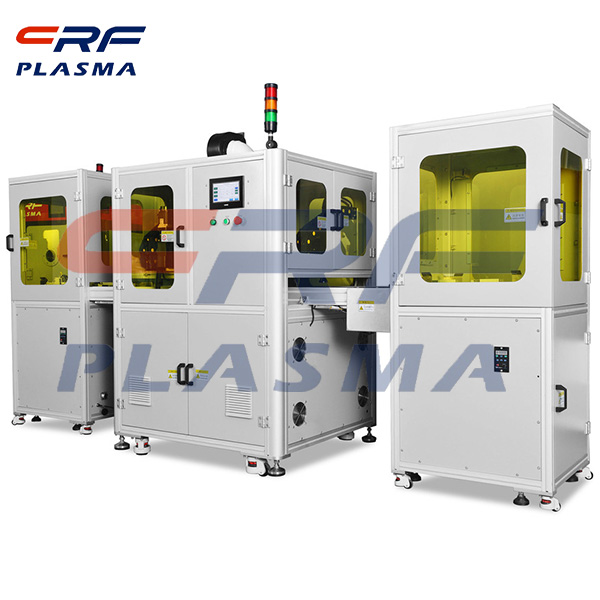
Other studies have shown that oxygen plasmas are more efficient for the etching of thick graphene. Oxygen plasmas are more efficient for the etching of litholene at a faster rate and are more effective for thicker layers of graphene. Graphics with lines and voids of 20μm were used to detect the etching effect. The graphene used in this study is 50nm thick and is grown on silicon dioxide. The etching conditions were a mixture of 70sccm oxygen and 30sccm argon, with a bias of 150W and a pressure of 55mT. The photoresistor used was the pattern obtained by twice spinning coated AZ4620 with a thickness of 20μm.
The etching rate for graphene is about 100nm/min, while the etching rate for photoresists AZ4620 is 330nm/min, which also requires thicker photoresists or the use of a 3-layer mask structure. Fortunately, the etching rate for amorphous carbon under this condition is about 20nm/min, which can be used as the resistance layer for graphene etching.
From the existing etching principle and experience analysis, mixing of oxygen plasma argon plasma not only ensure the strength of chemical etching can also be high bias to accelerate, with the heavier argon plasma bombardment graphene, ensure that the graphene films of relatively thick physical attacks, achieve etching, but apparently to remove residues, then it has no physical etching effect, And it will produce bombardment and damage to the film below. This means that a low bias oxygen plasma is used to complete the etching, which is both effective in removing the residue and protecting the underlying film. This scheme should be more efficient than using the main etching program to complete the etching, and get better graphics.
The above is the CRF plasma surface processor manufacturers of graphene etching principle experience analysis.
Scan the QR code to read on your phone

TEL:0755-3367 3020 / 0755-3367 3019

E-mail:sales-sfi@sfi-crf.com

ADD:Mabao Industrial Zone, Huangpu, Baoan District, Shenzhen


