Welcome to Shenzhen Sing Fung Intelligent Manufacturing Co., Ltd.
E-mail:shaobo@sfi-crf.com
Application of Plasma Surface Treatment in Microassembly Technology Application of Plasma Surface Treatment in Microassembly Technology
- Categories:Industry News
- Author:plasma cleaning machine-surface treatment equipment-CRF plasma machine-Sing Fung Intelligent Manufacturing
- Origin:
- Time of issue:2021-04-14
- Views:
(Summary description)Overview of microgroup assembly technology: From the beginning of micro assembly concept put forward, especially surface-mount technology development to a high level of specific stages, namely the guide feet must be less than 3 mm between components in surface-mount technology, with the further development of technology, now also refers to various forms of element SMT technology, such as circuit lead spacing is small, such as modules, components, systems or SMT technology. There is another saying that micro-assembly technology is short for micro-circuit assembly technology, that is, the assembler uses assembly equipment, tools, and micro-welding, interconnection and packaging technology to assemble a variety of micro components, integrated circuit chips, micro structural parts, etc., on the multi-layer interconnect substrate. Processes, methods and techniques for making it a highly reliable, high-density, two-dimensional microelectronic product (module/component/component/subsystem/system). The main application objects of micro - assembly technology are: micro - components, micro - spacing, micro - structure and micro - connection. The application of micro-assembly technology mainly includes: device level packaging, circuit module level assembly, micro-assembly or micro-system level assembly. The main contents of micro-assembly technology are as follows: 1) chip welding (conductive adhesive connection, eutectic welding, reverse assembly welding, etc.); 2) Interconnection of chemical plates (lead connection, automatic connection of carrier belt, micro-convex connection, etc.); 3) Device 3D assembly (wafer level 2D assembly, chip level 2D assembly, package level H-dimensional assembly); 4) Stereo assembly (chip level stereo assembly, board level stereo assembly). The main characteristics of microassembly technology are: 1) on a single printed plate (or substrate) to assemble a plurality of components (including outer package and no outer package) and other small components to form circuit modules (or components, Microsystems, subsystems); 2) the circuit module or component has a specific function and performance; 3) Independent circuit modules or components are generally not externally packaged, but can also be externally packaged (when the substrate is equipped with unpackaged components or specially required components); 4) Through motherboard and vertical interconnection technology, multiple independent circuit modules or components can be assembled into three-dimensional components -- dimensional three-dimensional assembly; 5) Multiple independent circuit modules or components can form a higher level system through motherboard, connection and plug interconnection or cable interconnection technology -- complete machine interconnection technology; 6) Multi-disciplinary optimization and micro-assembly design should be carried out according to the requirements of micro-assembly design with the pin spacing less than 3mm of the components. Plasma surface treatment process: In the process of microassembly, plasma surface treatment technology is a very important link, which directly affects the quality of the functional modules of microassembly. In the process of microassembly, plasma cleaning process is mainly used in the following two aspects. (1) point conductive adhesive before: the contaminants on the substrate will make the substrate wettability worse, point conductive adhesive is adverse to the tile glue, glue is round. Plasma surface treatment technology can greatly improve the wetting property of the substrate surface, which is beneficial to the adhesion between the conductive adhesive layer and the chip, and improve the bonding strength of the chip. (2) before the lead connection: chip affixed on the substrate, after high temperature curing, the substrate contaminants may contain particles and oxides, so that the lead and chip or substrate connection is not strong, resulting in insufficient connection strength. Isoionization treatment can obviously improve the surface activity before lead connection and thus enhance the strength of lead connection. The objects of plasma surface treatment in microassembly mainly include chip bonding zone, substrate, guide frame, ceramic substrate, etc. In this experiment, the substrate was cleaned, and silver and oxidation were generated on the surface of the substrate. Plasma cleaning machine was used to clean the substrate, and hydrogen and nitrogen mixture was selected as the cleaning process gas. During the cleaning process of plasma surface treatment, hydrogen plasma was effective enough to remove oxides on the substrate. The experimental results show that the process parameters such as pressure, power, time and gas flow can be effectively controlled in the cleaning process, and a better cleaning effect can be achieved.
Application of Plasma Surface Treatment in Microassembly Technology Application of Plasma Surface Treatment in Microassembly Technology
(Summary description)Overview of microgroup assembly technology:
From the beginning of micro assembly concept put forward, especially surface-mount technology development to a high level of specific stages, namely the guide feet must be less than 3 mm between components in surface-mount technology, with the further development of technology, now also refers to various forms of element SMT technology, such as circuit lead spacing is small, such as modules, components, systems or SMT technology. There is another saying that micro-assembly technology is short for micro-circuit assembly technology, that is, the assembler uses assembly equipment, tools, and micro-welding, interconnection and packaging technology to assemble a variety of micro components, integrated circuit chips, micro structural parts, etc., on the multi-layer interconnect substrate. Processes, methods and techniques for making it a highly reliable, high-density, two-dimensional microelectronic product (module/component/component/subsystem/system).
The main application objects of micro - assembly technology are: micro - components, micro - spacing, micro - structure and micro - connection.
The application of micro-assembly technology mainly includes: device level packaging, circuit module level assembly, micro-assembly or micro-system level assembly.
The main contents of micro-assembly technology are as follows: 1) chip welding (conductive adhesive connection, eutectic welding, reverse assembly welding, etc.); 2) Interconnection of chemical plates (lead connection, automatic connection of carrier belt, micro-convex connection, etc.); 3) Device 3D assembly (wafer level 2D assembly, chip level 2D assembly, package level H-dimensional assembly); 4) Stereo assembly (chip level stereo assembly, board level stereo assembly).
The main characteristics of microassembly technology are: 1) on a single printed plate (or substrate) to assemble a plurality of components (including outer package and no outer package) and other small components to form circuit modules (or components, Microsystems, subsystems); 2) the circuit module or component has a specific function and performance; 3) Independent circuit modules or components are generally not externally packaged, but can also be externally packaged (when the substrate is equipped with unpackaged components or specially required components); 4) Through motherboard and vertical interconnection technology, multiple independent circuit modules or components can be assembled into three-dimensional components -- dimensional three-dimensional assembly; 5) Multiple independent circuit modules or components can form a higher level system through motherboard, connection and plug interconnection or cable interconnection technology -- complete machine interconnection technology; 6) Multi-disciplinary optimization and micro-assembly design should be carried out according to the requirements of micro-assembly design with the pin spacing less than 3mm of the components.
Plasma surface treatment process:
In the process of microassembly, plasma surface treatment technology is a very important link, which directly affects the quality of the functional modules of microassembly. In the process of microassembly, plasma cleaning process is mainly used in the following two aspects.
(1) point conductive adhesive before: the contaminants on the substrate will make the substrate wettability worse, point conductive adhesive is adverse to the tile glue, glue is round. Plasma surface treatment technology can greatly improve the wetting property of the substrate surface, which is beneficial to the adhesion between the conductive adhesive layer and the chip, and improve the bonding strength of the chip.
(2) before the lead connection: chip affixed on the substrate, after high temperature curing, the substrate contaminants may contain particles and oxides, so that the lead and chip or substrate connection is not strong, resulting in insufficient connection strength. Isoionization treatment can obviously improve the surface activity before lead connection and thus enhance the strength of lead connection.
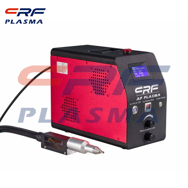
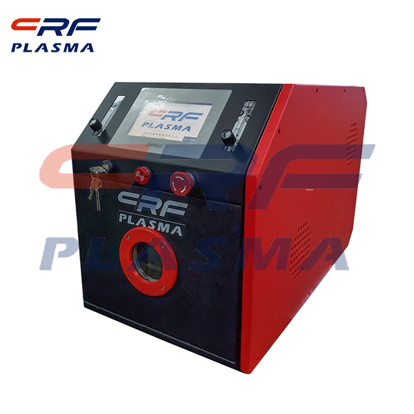
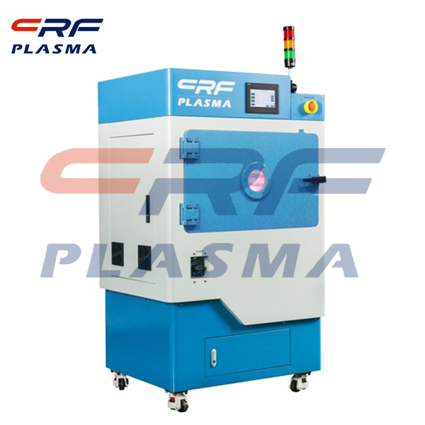
The objects of plasma surface treatment in microassembly mainly include chip bonding zone, substrate, guide frame, ceramic substrate, etc. In this experiment, the substrate was cleaned, and silver and oxidation were generated on the surface of the substrate. Plasma cleaning machine was used to clean the substrate, and hydrogen and nitrogen mixture was selected as the cleaning process gas. During the cleaning process of plasma surface treatment, hydrogen plasma was effective enough to remove oxides on the substrate. The experimental results show that the process parameters such as pressure, power, time and gas flow can be effectively controlled in the cleaning process, and a better cleaning effect can be achieved.
- Categories:Industry News
- Author:plasma cleaning machine-surface treatment equipment-CRF plasma machine-Sing Fung Intelligent Manufacturing
- Origin:
- Time of issue:2021-04-14 10:35
- Views:
Application of Plasma Surface Treatment in Microassembly Technology Application of Plasma Surface Treatment in Microassembly Technology:
Overview of microgroup assembly technology:
From the beginning of micro assembly concept put forward, especially surface-mount technology development to a high level of specific stages, namely the guide feet must be less than 3 mm between components in surface-mount technology, with the further development of technology, now also refers to various forms of element SMT technology, such as circuit lead spacing is small, such as modules, components, systems or SMT technology. There is another saying that micro-assembly technology is short for micro-circuit assembly technology, that is, the assembler uses assembly equipment, tools, and micro-welding, interconnection and packaging technology to assemble a variety of micro components, integrated circuit chips, micro structural parts, etc., on the multi-layer interconnect substrate. Processes, methods and techniques for making it a highly reliable, high-density, two-dimensional microelectronic product (module/component/component/subsystem/system).
The main application objects of micro - assembly technology are: micro - components, micro - spacing, micro - structure and micro - connection.
The application of micro-assembly technology mainly includes: device level packaging, circuit module level assembly, micro-assembly or micro-system level assembly.
The main contents of micro-assembly technology are as follows: 1) chip welding (conductive adhesive connection, eutectic welding, reverse assembly welding, etc.); 2) Interconnection of chemical plates (lead connection, automatic connection of carrier belt, micro-convex connection, etc.); 3) Device 3D assembly (wafer level 2D assembly, chip level 2D assembly, package level H-dimensional assembly); 4) Stereo assembly (chip level stereo assembly, board level stereo assembly).
The main characteristics of microassembly technology are: 1) on a single printed plate (or substrate) to assemble a plurality of components (including outer package and no outer package) and other small components to form circuit modules (or components, Microsystems, subsystems); 2) the circuit module or component has a specific function and performance; 3) Independent circuit modules or components are generally not externally packaged, but can also be externally packaged (when the substrate is equipped with unpackaged components or specially required components); 4) Through motherboard and vertical interconnection technology, multiple independent circuit modules or components can be assembled into three-dimensional components -- dimensional three-dimensional assembly; 5) Multiple independent circuit modules or components can form a higher level system through motherboard, connection and plug interconnection or cable interconnection technology -- complete machine interconnection technology; 6) Multi-disciplinary optimization and micro-assembly design should be carried out according to the requirements of micro-assembly design with the pin spacing less than 3mm of the components.
Plasma surface treatment process:
In the process of microassembly, plasma surface treatment technology is a very important link, which directly affects the quality of the functional modules of microassembly. In the process of microassembly, plasma cleaning process is mainly used in the following two aspects.
(1) point conductive adhesive before: the contaminants on the substrate will make the substrate wettability worse, point conductive adhesive is adverse to the tile glue, glue is round. Plasma surface treatment technology can greatly improve the wetting property of the substrate surface, which is beneficial to the adhesion between the conductive adhesive layer and the chip, and improve the bonding strength of the chip.
(2) before the lead connection: chip affixed on the substrate, after high temperature curing, the substrate contaminants may contain particles and oxides, so that the lead and chip or substrate connection is not strong, resulting in insufficient connection strength. Isoionization treatment can obviously improve the surface activity before lead connection and thus enhance the strength of lead connection.
The objects of plasma surface treatment in microassembly mainly include chip bonding zone, substrate, guide frame, ceramic substrate, etc. In this experiment, the substrate was cleaned, and silver and oxidation were generated on the surface of the substrate. Plasma cleaning machine was used to clean the substrate, and hydrogen and nitrogen mixture was selected as the cleaning process gas. During the cleaning process of plasma surface treatment, hydrogen plasma was effective enough to remove oxides on the substrate. The experimental results show that the process parameters such as pressure, power, time and gas flow can be effectively controlled in the cleaning process, and a better cleaning effect can be achieved.
Scan the QR code to read on your phone

TEL:0755-3367 3020 / 0755-3367 3019

E-mail:sales-sfi@sfi-crf.com

ADD:Mabao Industrial Zone, Huangpu, Baoan District, Shenzhen


