

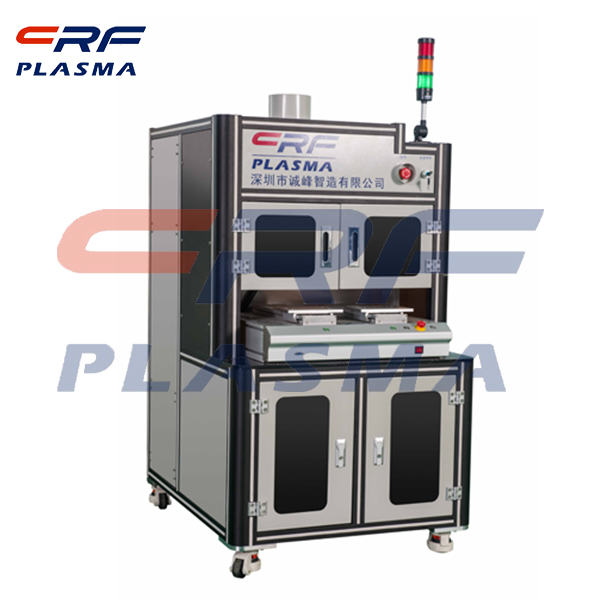
Welcome to Shenzhen Sing Fung Intelligent Manufacturing Co., Ltd.
E-mail:shaobo@sfi-crf.com


News
Domestic plasma etching machine manufacturers: directed self-assembly material plasma etching
- Categories:Industry News
- Author:plasma cleaning machine-surface treatment equipment-CRF plasma machine-Sing Fung Intelligent Manufacturing
- Origin:
- Time of issue:2021-04-27
- Views:
(Summary description)Domestic plasma etching machine manufacturers: directed self-assembly material plasma etching Domestic Plasma Etching Machine Manufactory Directional Self-assembly Plasma Etching Application: In the process below 22nm, it is necessary to reduce the periodic spacing. The general practice is to achieve the pattern definition of small size and small diameter through the way of secondary exposure, namely repeated lithography etching. This method has been successfully mass-produced in the fin type field effect transistor, but it will undoubtedly increase exponentially. Many experts in the field of micrographic definition have long been exploring alternative methods of micrographic definition that go beyond the current lithography physics. Among them, directional self-assembly using polystyrene (PS), polymethyl methacrylate (PMMA) and its block copolymer is a method that has been discussed more. The method is to use the phase transition conditions between different components in the block copolymer to remove part of the components to realize the pattern definition. Some successful cases are the use of block copolymers of polystyrene and polymethyl methacrylate to reduce periodic spacing and the realization of minimal diameter contact holes through graphic definition. The minimum contact hole is defined by first defining the graph and then filling the block copolymer, so that the block copolymer will fill the previously defined graph, and the phase transition occurs at the boundary of the graph first and then gradually spreads to the body, which is just for our use. If the diameter of the contact hole is defined as 68nm first, then the contact hole can be reduced to 20nm after the second definition in this way. At the same time, different shapes, sizes and even different intensities of contact holes can be realized by using the different morphologies of the patterns in the previous step and adjusting the morphology of block copolymer. Domestic plasma etching machine manufacturer If the graphical definition of directional self-assembly can be used in mass production, how to remove these unwanted block copolymers becomes a problem that must be further studied. At present, the general method is to remove by wet etching or dry plasma etching. Generally speaking, the selection ratio of wet removal is very high, but the definition of the figure is not good enough, which will bring poor line width roughness and may cause the collapse of dense and narrow lines, due to the wetting effect of the solution. And domestic plasma etching machine manufacturers dry plasma etching removal generally lower selection ratio but will not have these problems. Common dry etching methods and actual performance are listed in Table 8.3. It can be seen that the mixed etching effect of AR and oxygen is good. Although the selection ratio of block copolymer is not high, the selection ratio of the lower material, the line width roughness and the key size definition are all good. Table 8.3 Etching results of block copolymers with different gas ratios: Ar O2 Ar/O2 CF4 O2/CHF3 PMMA/PS etch selectivity 3.63 1.50 2.04 1.85 1.82 Etch sel. To underlying material(Si or SiOx) Good Good Better Poor Poor Edge roughness Poor Poor Good Good Good CD(original CD:~25nm) Deformed 21.58 nm 24.24 nm 26.50 nm 25.92 nm Xe and H2 have a higher etching rate for PMMA and PS, the thicker PMMA/PS films growing on the control plate will be completed by plasma etching faster, and the etching termination phenomenon will occur when the two materials are etched with CO, and the gas saturation phenomenon occurs at the beginning of the etching stage. Compared with H2, the etching rate of PS will be faster and the selection ratio will be lower. And CO will be deposited on the PS surface can be used to adjust the etching selection ratio. Using the mixture of these three gases, we can see that the selection ratio is all above 5, which can be applied to industrial production. However, XE-Co mixture will cause more carbides to deposit on the surface of PMMA, which will destroy the original pattern. In contrast, the combination of Co-H2 has little influence on the patterning and is conducive to the actual control. Co-H2 has been used to successfully form lithographic plasma etching contact holes with key size difference less than 1nm and diameter of 15nm in a 10nm process. More and more close to the bottleneck of silicon semiconductor, new materials continue to emerge, and the realization of the device is more and more, and closer to mass production. These new materials, which will soon appear in semiconductor integrated circuits, are very challenging for etching. This kind of material generally has better electrical conductivity and chemical activity, preferring a little more chemical etching. The general requirement is that the graphic definition should be accurate and the damage to the key layer and the contact layer should be small. On this basi
Domestic plasma etching machine manufacturers: directed self-assembly material plasma etching
(Summary description)Domestic plasma etching machine manufacturers: directed self-assembly material plasma etching
Domestic Plasma Etching Machine Manufactory Directional Self-assembly Plasma Etching Application:
In the process below 22nm, it is necessary to reduce the periodic spacing. The general practice is to achieve the pattern definition of small size and small diameter through the way of secondary exposure, namely repeated lithography etching. This method has been successfully mass-produced in the fin type field effect transistor, but it will undoubtedly increase exponentially. Many experts in the field of micrographic definition have long been exploring alternative methods of micrographic definition that go beyond the current lithography physics. Among them, directional self-assembly using polystyrene (PS), polymethyl methacrylate (PMMA) and its block copolymer is a method that has been discussed more. The method is to use the phase transition conditions between different components in the block copolymer to remove part of the components to realize the pattern definition. Some successful cases are the use of block copolymers of polystyrene and polymethyl methacrylate to reduce periodic spacing and the realization of minimal diameter contact holes through graphic definition. The minimum contact hole is defined by first defining the graph and then filling the block copolymer, so that the block copolymer will fill the previously defined graph, and the phase transition occurs at the boundary of the graph first and then gradually spreads to the body, which is just for our use. If the diameter of the contact hole is defined as 68nm first, then the contact hole can be reduced to 20nm after the second definition in this way. At the same time, different shapes, sizes and even different intensities of contact holes can be realized by using the different morphologies of the patterns in the previous step and adjusting the morphology of block copolymer.
Domestic plasma etching machine manufacturer
If the graphical definition of directional self-assembly can be used in mass production, how to remove these unwanted block copolymers becomes a problem that must be further studied. At present, the general method is to remove by wet etching or dry plasma etching. Generally speaking, the selection ratio of wet removal is very high, but the definition of the figure is not good enough, which will bring poor line width roughness and may cause the collapse of dense and narrow lines, due to the wetting effect of the solution. And domestic plasma etching machine manufacturers dry plasma etching removal generally lower selection ratio but will not have these problems. Common dry etching methods and actual performance are listed in Table 8.3. It can be seen that the mixed etching effect of AR and oxygen is good. Although the selection ratio of block copolymer is not high, the selection ratio of the lower material, the line width roughness and the key size definition are all good.
Table 8.3 Etching results of block copolymers with different gas ratios:
Ar
O2
Ar/O2
CF4
O2/CHF3
PMMA/PS etch selectivity
3.63
1.50
2.04
1.85
1.82
Etch sel. To underlying material(Si or SiOx)
Good
Good
Better
Poor
Poor
Edge roughness
Poor
Poor
Good
Good
Good
CD(original CD:~25nm)
Deformed
21.58 nm
24.24 nm
26.50 nm
25.92 nm
Xe and H2 have a higher etching rate for PMMA and PS, the thicker PMMA/PS films growing on the control plate will be completed by plasma etching faster, and the etching termination phenomenon will occur when the two materials are etched with CO, and the gas saturation phenomenon occurs at the beginning of the etching stage. Compared with H2, the etching rate of PS will be faster and the selection ratio will be lower. And CO will be deposited on the PS surface can be used to adjust the etching selection ratio. Using the mixture of these three gases, we can see that the selection ratio is all above 5, which can be applied to industrial production. However, XE-Co mixture will cause more carbides to deposit on the surface of PMMA, which will destroy the original pattern. In contrast, the combination of Co-H2 has little influence on the patterning and is conducive to the actual control. Co-H2 has been used to successfully form lithographic plasma etching contact holes with key size difference less than 1nm and diameter of 15nm in a 10nm process.
More and more close to the bottleneck of silicon semiconductor, new materials continue to emerge, and the realization of the device is more and more, and closer to mass production. These new materials, which will soon appear in semiconductor integrated circuits, are very challenging for etching. This kind of material generally has better electrical conductivity and chemical activity, preferring a little more chemical etching. The general requirement is that the graphic definition should be accurate and the damage to the key layer and the contact layer should be small. On this basi
- Categories:Industry News
- Author:plasma cleaning machine-surface treatment equipment-CRF plasma machine-Sing Fung Intelligent Manufacturing
- Origin:
- Time of issue:2021-04-27 08:31
- Views:
Information
Domestic plasma etching machine manufacturers: directed self-assembly material plasma etching
Domestic Plasma Etching Machine Manufactory Directional Self-assembly Plasma Etching Application:
In the process below 22nm, it is necessary to reduce the periodic spacing. The general practice is to achieve the pattern definition of small size and small diameter through the way of secondary exposure, namely repeated lithography etching. This method has been successfully mass-produced in the fin type field effect transistor, but it will undoubtedly increase exponentially. Many experts in the field of micrographic definition have long been exploring alternative methods of micrographic definition that go beyond the current lithography physics. Among them, directional self-assembly using polystyrene (PS), polymethyl methacrylate (PMMA) and its block copolymer is a method that has been discussed more. The method is to use the phase transition conditions between different components in the block copolymer to remove part of the components to realize the pattern definition. Some successful cases are the use of block copolymers of polystyrene and polymethyl methacrylate to reduce periodic spacing and the realization of minimal diameter contact holes through graphic definition. The minimum contact hole is defined by first defining the graph and then filling the block copolymer, so that the block copolymer will fill the previously defined graph, and the phase transition occurs at the boundary of the graph first and then gradually spreads to the body, which is just for our use. If the diameter of the contact hole is defined as 68nm first, then the contact hole can be reduced to 20nm after the second definition in this way. At the same time, different shapes, sizes and even different intensities of contact holes can be realized by using the different morphologies of the patterns in the previous step and adjusting the morphology of block copolymer.
Domestic plasma etching machine manufacturer
If the graphical definition of directional self-assembly can be used in mass production, how to remove these unwanted block copolymers becomes a problem that must be further studied. At present, the general method is to remove by wet etching or dry plasma etching. Generally speaking, the selection ratio of wet removal is very high, but the definition of the figure is not good enough, which will bring poor line width roughness and may cause the collapse of dense and narrow lines, due to the wetting effect of the solution. And domestic plasma etching machine manufacturers dry plasma etching removal generally lower selection ratio but will not have these problems. Common dry etching methods and actual performance are listed in Table 8.3. It can be seen that the mixed etching effect of AR and oxygen is good. Although the selection ratio of block copolymer is not high, the selection ratio of the lower material, the line width roughness and the key size definition are all good.
Table 8.3 Etching results of block copolymers with different gas ratios:
Ar
O2
Ar/O2
CF4
O2/CHF3
PMMA/PS etch selectivity
3.63
1.50
2.04
1.85
1.82
Etch sel. To underlying material(Si or SiOx)
Good
Good
Better
Poor
Poor
Edge roughness
Poor
Poor
Good
Good
Good
CD(original CD:~25nm)
Deformed
21.58 nm
24.24 nm
26.50 nm
25.92 nm
Xe and H2 have a higher etching rate for PMMA and PS, the thicker PMMA/PS films growing on the control plate will be completed by plasma etching faster, and the etching termination phenomenon will occur when the two materials are etched with CO, and the gas saturation phenomenon occurs at the beginning of the etching stage. Compared with H2, the etching rate of PS will be faster and the selection ratio will be lower. And CO will be deposited on the PS surface can be used to adjust the etching selection ratio. Using the mixture of these three gases, we can see that the selection ratio is all above 5, which can be applied to industrial production. However, XE-Co mixture will cause more carbides to deposit on the surface of PMMA, which will destroy the original pattern. In contrast, the combination of Co-H2 has little influence on the patterning and is conducive to the actual control. Co-H2 has been used to successfully form lithographic plasma etching contact holes with key size difference less than 1nm and diameter of 15nm in a 10nm process.
More and more close to the bottleneck of silicon semiconductor, new materials continue to emerge, and the realization of the device is more and more, and closer to mass production. These new materials, which will soon appear in semiconductor integrated circuits, are very challenging for etching. This kind of material generally has better electrical conductivity and chemical activity, preferring a little more chemical etching. The general requirement is that the graphic definition should be accurate and the damage to the key layer and the contact layer should be small. On this basis, the high selection ratio of the mask layer and the lower material should be pursued. Of course, for more and more sophisticated device processing, the definition of special pattern is more and more cases, for these two types of cases, new plasma etching machine and new etching method is the effective way.
The above is the introduction of plasma etching of directional self-assembly materials by the manufacturers of plasma etching. I hope it will be helpful to you
Keyword:
Scan the QR code to read on your phone
Relevant Information

Small vacuum plasma cleaning machine vacuum plasma cleaning surface material modification
2021-04-26 08:35

Plasma equipment manufacturer Chengfeng Zhizao professional research and development design of plasma technology
2021-04-24 17:17

Small vacuum plasma cleaning machine vacuum plasma cleaning surface material modification
2021-04-24 17:07

Influence of plasma surface treatment on sensing performance of flexible conductive fiber
2021-04-23 16:15


Factors influencing the cleaning effect of copper support treated by copper surface plasma
2021-04-21 15:22

Plasma surface activation environmental protection equipment process applied to silica gel products
2021-04-21 15:19


TEL:0755-3367 3020 / 0755-3367 3019

E-mail:sales-sfi@sfi-crf.com

ADD:Mabao Industrial Zone, Huangpu, Baoan District, Shenzhen

