

Welcome to Shenzhen Sing Fung Intelligent Manufacturing Co., Ltd.
E-mail:shaobo@sfi-crf.com


IC semiconductor field
- Categories:IC semiconductor field
- Author:
- Origin:
- Time of issue:2020-07-28
- Views:
(Summary description)With the rapid development of smart phones, people’s requirements for mobile phone camera pixels are getting higher and higher.

IC semiconductor field
(Summary description)With the rapid development of smart phones, people’s requirements for mobile phone camera pixels are getting higher and higher.
- Categories:IC semiconductor field
- Author:
- Origin:
- Time of issue:2020-07-28 09:32
- Views:
Information
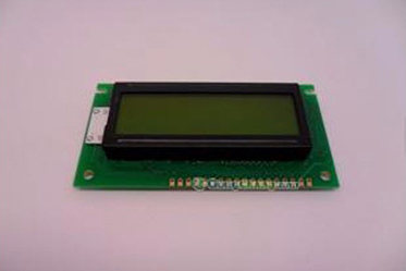
1. COB/COF/COG
With the rapid development of smart phones, people’s requirements for mobile phone camera pixels are getting higher and higher. Nowadays, the pixels of mobile phone camera module manufactured with traditional CSP packaging process can no longer meet people’s needs, and COB/COG/COF packaging is used. Process-manufactured mobile phone camera modules have been widely used in current multi-megapixel mobile phones, but their manufacturing yield is often only about 85% due to their process characteristics, and the main reason for the low yield rate of mobile phones is Centrifugal cleaning machine and ultrasonic cleaning can not clean the surface of holder and Pad with high cleanliness, resulting in low adhesion between holder and IR and poor bonding. After plasma treatment, the organic pollutants on holder can be removed. Activating the base material can increase its adhesion to IR by two or three times. It can also remove oxides on the surface of the Pad and roughen the surface, which significantly improves the first-time success rate of banding.
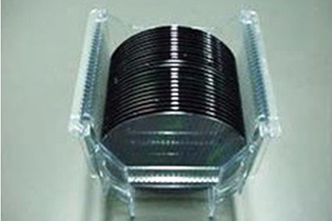
2. Semiconductor Wafer
In the field of IC chip manufacturing, plasma treatment technology has become an irreplaceable mature process, whether in the implantation of chip source ions, the coating of wafers, or our low-temperature plasma surface treatment equipment can achieve: The removal of oxide film, organic matter, masking and other purification treatments on the surface of the wafer and surface activation improve the wettability of the wafer surface.
Scan the QR code to read on your phone
Previous:
None
Next:
None
Previous:
None
Next:
None


TEL:0755-3367 3020 / 0755-3367 3019

E-mail:sales-sfi@sfi-crf.com

ADD:Mabao Industrial Zone, Huangpu, Baoan District, Shenzhen

