

Welcome to Shenzhen Sing Fung Intelligent Manufacturing Co., Ltd.
E-mail:shaobo@sfi-crf.com


News
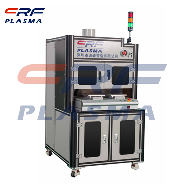
Wide width plasma surface processor plasma Cleaning integrated circuit manufacturing
- Categories:Technical Support
- Author:plasma cleaning machine-surface treatment equipment-CRF plasma machine-Sing Fung Intelligent Manufacturing
- Origin:
- Time of issue:2020-12-15
- Views:
(Summary description)As the volume of manufacturing integrated circuits decreases, the size of lead bonding pads decreases, leading to increased potential contamination of pads. When the wire bonding pad is polluted, the tensile strength of the bonding pad decreases and the uniformity of the connection strength decreases. It is therefore important to remove contaminants from the bonding pad prior to lead bonding. The plasma cleaning technology of wide width plasma surface processor driven by RF can be used to prepare the solder pad before lead bonding. Wideband plasma surface treatment technology is used to clean the surface of the device in order to improve the tensile strength of the lead, thus reducing the fault of the device and increasing the pass rate. The quality of lead bonding in integrated circuits has great influence on the reliability of microelectronic devices. The bonding area must be free of pollution and have good bonding performance. The presence of pollutants such as oxides and organic residues will seriously weaken the tensile strength of lead bonding. By using the wide-width plasma surface processor, the dirt produced in the process can be thoroughly removed, so as to effectively remove the dirt, and make the dirt surface activated, significantly improve the bonding strength of lead, effectively improve the reliability of integrated circuit devices. The plasma cleaning treatment of chip and package substrate in integrated circuit can effectively improve the surface activity of the substrate, greatly improve the bonding strength, reduce the lamination of chip and substrate, improve the thermal conductivity, improve the reliability and stability of integrated circuit, and improve the service life of the product. By using the plasma cleaning technology, the processing technology of IC can be improved and the quality of the products can be improved effectively. With the application of plasma surface treatment technology, we have more and better ways to treat materials! Believe in technology, believe in the future.
Wide width plasma surface processor plasma Cleaning integrated circuit manufacturing
(Summary description)As the volume of manufacturing integrated circuits decreases, the size of lead bonding pads decreases, leading to increased potential contamination of pads. When the wire bonding pad is polluted, the tensile strength of the bonding pad decreases and the uniformity of the connection strength decreases. It is therefore important to remove contaminants from the bonding pad prior to lead bonding.
The plasma cleaning technology of wide width plasma surface processor driven by RF can be used to prepare the solder pad before lead bonding. Wideband plasma surface treatment technology is used to clean the surface of the device in order to improve the tensile strength of the lead, thus reducing the fault of the device and increasing the pass rate.
The quality of lead bonding in integrated circuits has great influence on the reliability of microelectronic devices. The bonding area must be free of pollution and have good bonding performance. The presence of pollutants such as oxides and organic residues will seriously weaken the tensile strength of lead bonding. By using the wide-width plasma surface processor, the dirt produced in the process can be thoroughly removed, so as to effectively remove the dirt, and make the dirt surface activated, significantly improve the bonding strength of lead, effectively improve the reliability of integrated circuit devices.
The plasma cleaning treatment of chip and package substrate in integrated circuit can effectively improve the surface activity of the substrate, greatly improve the bonding strength, reduce the lamination of chip and substrate, improve the thermal conductivity, improve the reliability and stability of integrated circuit, and improve the service life of the product.
By using the plasma cleaning technology, the processing technology of IC can be improved and the quality of the products can be improved effectively. With the application of plasma surface treatment technology, we have more and better ways to treat materials! Believe in technology, believe in the future.
- Categories:Technical Support
- Author:plasma cleaning machine-surface treatment equipment-CRF plasma machine-Sing Fung Intelligent Manufacturing
- Origin:
- Time of issue:2020-12-15 10:11
- Views:
Information
Wide width plasma surface processor plasma Cleaning integrated circuit manufacturing:
As the volume of manufacturing integrated circuits decreases, the size of lead bonding pads decreases, leading to increased potential contamination of pads. When the wire bonding pad is polluted, the tensile strength of the bonding pad decreases and the uniformity of the connection strength decreases. It is therefore important to remove contaminants from the bonding pad prior to lead bonding.
The plasma cleaning technology of wide width plasma surface processor driven by RF can be used to prepare the solder pad before lead bonding. Wideband plasma surface treatment technology is used to clean the surface of the device in order to improve the tensile strength of the lead, thus reducing the fault of the device and increasing the pass rate.
The quality of lead bonding in integrated circuits has great influence on the reliability of microelectronic devices. The bonding area must be free of pollution and have good bonding performance. The presence of pollutants such as oxides and organic residues will seriously weaken the tensile strength of lead bonding. By using the wide-width plasma surface processor, the dirt produced in the process can be thoroughly removed, so as to effectively remove the dirt, and make the dirt surface activated, significantly improve the bonding strength of lead, effectively improve the reliability of integrated circuit devices.
The plasma cleaning treatment of chip and package substrate in integrated circuit can effectively improve the surface activity of the substrate, greatly improve the bonding strength, reduce the lamination of chip and substrate, improve the thermal conductivity, improve the reliability and stability of integrated circuit, and improve the service life of the product.
By using the plasma cleaning technology, the processing technology of IC can be improved and the quality of the products can be improved effectively. With the application of plasma surface treatment technology, we have more and better ways to treat materials! Believe in technology, believe in the future.
Scan the QR code to read on your phone
Relevant Information


Verification of the effect of plasma cleaning machine for wide-width plasma equipment
2020-12-14 10:42

Application of plasma device Stress Proximity technology in semiconductor Technology
2020-12-14 10:38


TEL:0755-3367 3020 / 0755-3367 3019

E-mail:sales-sfi@sfi-crf.com

ADD:Mabao Industrial Zone, Huangpu, Baoan District, Shenzhen

