

Welcome to Shenzhen Sing Fung Intelligent Manufacturing Co., Ltd.
E-mail:shaobo@sfi-crf.com


News
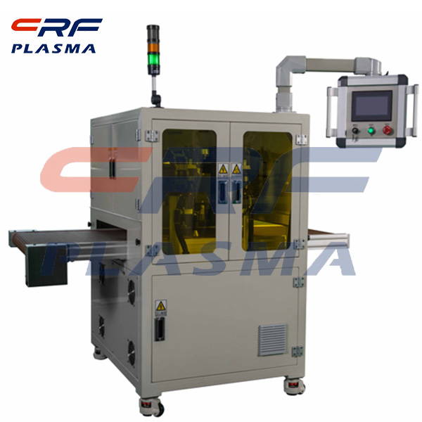
Plasma etching machine process introduction
- Categories:Company Dynamics
- Author:plasma cleaning machine-surface treatment equipment-CRF plasma machine-Sing Fung Intelligent Manufacturing
- Origin:
- Time of issue:2020-11-07
- Views:
(Summary description)Plasma etching machine etching can be divided into two processes: first, the chemical active components of the plasma, these active components react with solid material substances, produce volatile compounds, and diffuse to the surface, discharge. Take CF4 as an example, its dissociation F reacts with S to form SiF4 gas, forming micro-milling structure on the surface of Si material. Plasma etching refers to ion etching, sputtering etching and plasma ashing. The modification depth of plasma etcher depends on the substrate temperature, treatment time and material diffusion characteristics, while the modification type depends on the substrate and process parameters. Plasmas can only be etched a few microns deep on the surface and the surface properties change, but the surface properties of most materials can be maintained. The technology can also be used for surface cleaning, curing, coarsening, changing hydrophilicity and adhesion, etc., as well as for the manufacture of semiconductor integrated circuits, where sample thinning can be observed under an electron microscope. Chemical reactions can produce volatile products by chemical sputtering. Common gases include Ar, He, O2, H2, H2O, CO2, Cl2, F2 and organic vapour. Inert ion sputtering is closer to the physical process than plasma sputtering with chemical reaction. Plasma F etching Si is widely used in semiconductor equipment manufacturing. The three steps of etching reaction are as follows: Chemical adsorption: F2→F2 (ADS) →2F (ADS) Reaction: Si+4F (ADS) →SiF4 (ADS) Desorption: SiF4 (ADS) →SiF4 (GAS) In the etching process, the high-density plasma source has many advantages, such as more accurate control of workpiece size, higher etching rate and better material selectivity. The high density plasma source can work under low voltage, so the oscillation of sheath can be weakened. In the process of chip etching, plasma source etching with high density is used, and independent rf source is needed to bias the wafer, so that energy and ions are independent of each other. Since the energy of ions is generally in the order of several electron volts, when ions enter the negative sheath, they will reach hundreds of electron volts through energy acceleration and have high directivity, thus making ion etching anisotropic.
Plasma etching machine process introduction
(Summary description)Plasma etching machine etching can be divided into two processes: first, the chemical active components of the plasma, these active components react with solid material substances, produce volatile compounds, and diffuse to the surface, discharge. Take CF4 as an example, its dissociation F reacts with S to form SiF4 gas, forming micro-milling structure on the surface of Si material. Plasma etching refers to ion etching, sputtering etching and plasma ashing.
The modification depth of plasma etcher depends on the substrate temperature, treatment time and material diffusion characteristics, while the modification type depends on the substrate and process parameters. Plasmas can only be etched a few microns deep on the surface and the surface properties change, but the surface properties of most materials can be maintained. The technology can also be used for surface cleaning, curing, coarsening, changing hydrophilicity and adhesion, etc., as well as for the manufacture of semiconductor integrated circuits, where sample thinning can be observed under an electron microscope. Chemical reactions can produce volatile products by chemical sputtering. Common gases include Ar, He, O2, H2, H2O, CO2, Cl2, F2 and organic vapour. Inert ion sputtering is closer to the physical process than plasma sputtering with chemical reaction.
Plasma F etching Si is widely used in semiconductor equipment manufacturing. The three steps of etching reaction are as follows:
Chemical adsorption: F2→F2 (ADS) →2F (ADS)
Reaction: Si+4F (ADS) →SiF4 (ADS)
Desorption: SiF4 (ADS) →SiF4 (GAS)
In the etching process, the high-density plasma source has many advantages, such as more accurate control of workpiece size, higher etching rate and better material selectivity. The high density plasma source can work under low voltage, so the oscillation of sheath can be weakened. In the process of chip etching, plasma source etching with high density is used, and independent rf source is needed to bias the wafer, so that energy and ions are independent of each other. Since the energy of ions is generally in the order of several electron volts, when ions enter the negative sheath, they will reach hundreds of electron volts through energy acceleration and have high directivity, thus making ion etching anisotropic.
- Categories:Company Dynamics
- Author:plasma cleaning machine-surface treatment equipment-CRF plasma machine-Sing Fung Intelligent Manufacturing
- Origin:
- Time of issue:2020-11-07 09:04
- Views:
Information
Plasma etching machine process introduction:
Plasma etching machine etching can be divided into two processes: first, the chemical active components of the plasma, these active components react with solid material substances, produce volatile compounds, and diffuse to the surface, discharge. Take CF4 as an example, its dissociation F reacts with S to form SiF4 gas, forming micro-milling structure on the surface of Si material. Plasma etching refers to ion etching, sputtering etching and plasma ashing.
The modification depth of plasma etcher depends on the substrate temperature, treatment time and material diffusion characteristics, while the modification type depends on the substrate and process parameters. Plasmas can only be etched a few microns deep on the surface and the surface properties change, but the surface properties of most materials can be maintained. The technology can also be used for surface cleaning, curing, coarsening, changing hydrophilicity and adhesion, etc., as well as for the manufacture of semiconductor integrated circuits, where sample thinning can be observed under an electron microscope. Chemical reactions can produce volatile products by chemical sputtering. Common gases include Ar, He, O2, H2, H2O, CO2, Cl2, F2 and organic vapour. Inert ion sputtering is closer to the physical process than plasma sputtering with chemical reaction.
Plasma F etching Si is widely used in semiconductor equipment manufacturing. The three steps of etching reaction are as follows:
Chemical adsorption: F2→F2 (ADS) →2F (ADS)
Reaction: Si+4F (ADS) →SiF4 (ADS)
Desorption: SiF4 (ADS) →SiF4 (GAS)
In the etching process, the high-density plasma source has many advantages, such as more accurate control of workpiece size, higher etching rate and better material selectivity. The high density plasma source can work under low voltage, so the oscillation of sheath can be weakened. In the process of chip etching, plasma source etching with high density is used, and independent rf source is needed to bias the wafer, so that energy and ions are independent of each other. Since the energy of ions is generally in the order of several electron volts, when ions enter the negative sheath, they will reach hundreds of electron volts through energy acceleration and have high directivity, thus making ion etching anisotropic.
Scan the QR code to read on your phone
Relevant Information

Atmospheric pressure plasma cleaning ritualistic reaction process diagnosis technology
2020-11-07 08:56


Plasma cleaning instrument Atmospheric pressure DIELECTRIC barrier discharge plasma
2020-11-05 09:42


TEL:0755-3367 3020 / 0755-3367 3019

E-mail:sales-sfi@sfi-crf.com

ADD:Mabao Industrial Zone, Huangpu, Baoan District, Shenzhen

