

Welcome to Shenzhen Sing Fung Intelligent Manufacturing Co., Ltd.
E-mail:shaobo@sfi-crf.com


News
Manufacturing application of semiconductor plasma cleaning machine
- Categories:Technical Support
- Author:plasma cleaning machine-surface treatment equipment-CRF plasma machine-Sing Fung Intelligent Manufacturing
- Origin:
- Time of issue:2020-10-22
- Views:
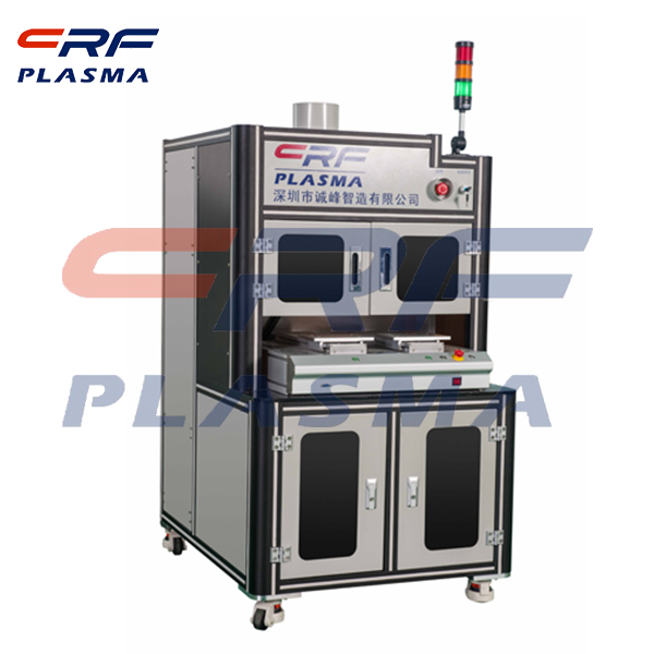
(Summary description)Plasma assisted cleaning technology is a kind of precision cleaning technology in advanced manufacturing industry, which can be widely used in many industries. The following is to introduce the application of plasma cleaning technology in semiconductor manufacturing industry. Chemical vapor deposition (CVD) and etching are widely used in semiconductor processing. CVD can be used in the deposition of polysilicon thin films, silicon nitride thin films, silicon dioxide thin films, tungsten and other metal thin films. In addition, CVD technology is also used to connect the micro - three - stage pipe and the thin conductor in the circuit. After the CVD reaction, some residues will deposit in the inner wall of the CVD reaction chamber. The danger here is that these residues will escape from the inner wall and contaminate the subsequent circulation process. Therefore, before the new deposition process begins, the CVD chamber needs to be cleaned with a plasma cleaning machine to maintain the qualified product output. Commonly used cleaning gas is F containing gas such as PFCs and SF6, which can be used as plasma generated gas to clean Sio2 or Si3N4 on the wall of CVD chamber. During the recirculation process, the F atomic energy decomposed by FFC under the action of plasma etched the electrode, the residue on the chamber wall, and the residue on the hardware devices in the chamber. In the plasma cleaning machine cleaning process, a considerable part of the FFC in the chamber did not dissociate into active F atoms. Unless emission reduction technology is adopted, this unreacted gas containing F will eventually escape into the atmosphere. Since these gases are present in the atmosphere for a long time, contributing significantly to global warming and producing four orders of magnitude more heat than carbon dioxide, the International Environment Organization has been developing technologies to reduce their emissions since 1994. Nitrogen has little influence on greenhouse effect and can replace the gas containing F above. Another step in the semiconductor industry is to use a plasma cleaner to clean photoresist made of photosensitive organic material on the surface of the element on the silicone sheet. Before the start of the precipitation process, the remnants of photoresist must be clean, using hot sulfuric acid and hydrogen peroxide solution or other toxic organic solvent to degumming of colloid, it leads to environmental problem, but using plasma cleaning machine to clean, can use the gases such as sulfur trioxide degumming, thus reducing the dependence on chemical solvents and organic solvent. For general manufacturers, the use of plasma to remove adhesive technology, chemical solution can be reduced by more than a thousand times, not only environmental protection, and save a lot of money for enterprises.
Manufacturing application of semiconductor plasma cleaning machine
(Summary description)Plasma assisted cleaning technology is a kind of precision cleaning technology in advanced manufacturing industry, which can be widely used in many industries. The following is to introduce the application of plasma cleaning technology in semiconductor manufacturing industry.
Chemical vapor deposition (CVD) and etching are widely used in semiconductor processing. CVD can be used in the deposition of polysilicon thin films, silicon nitride thin films, silicon dioxide thin films, tungsten and other metal thin films. In addition, CVD technology is also used to connect the micro - three - stage pipe and the thin conductor in the circuit.
After the CVD reaction, some residues will deposit in the inner wall of the CVD reaction chamber. The danger here is that these residues will escape from the inner wall and contaminate the subsequent circulation process. Therefore, before the new deposition process begins, the CVD chamber needs to be cleaned with a plasma cleaning machine to maintain the qualified product output. Commonly used cleaning gas is F containing gas such as PFCs and SF6, which can be used as plasma generated gas to clean Sio2 or Si3N4 on the wall of CVD chamber. During the recirculation process, the F atomic energy decomposed by FFC under the action of plasma etched the electrode, the residue on the chamber wall, and the residue on the hardware devices in the chamber.
In the plasma cleaning machine cleaning process, a considerable part of the FFC in the chamber did not dissociate into active F atoms. Unless emission reduction technology is adopted, this unreacted gas containing F will eventually escape into the atmosphere. Since these gases are present in the atmosphere for a long time, contributing significantly to global warming and producing four orders of magnitude more heat than carbon dioxide, the International Environment Organization has been developing technologies to reduce their emissions since 1994. Nitrogen has little influence on greenhouse effect and can replace the gas containing F above.
Another step in the semiconductor industry is to use a plasma cleaner to clean photoresist made of photosensitive organic material on the surface of the element on the silicone sheet. Before the start of the precipitation process, the remnants of photoresist must be clean, using hot sulfuric acid and hydrogen peroxide solution or other toxic organic solvent to degumming of colloid, it leads to environmental problem, but using plasma cleaning machine to clean, can use the gases such as sulfur trioxide degumming, thus reducing the dependence on chemical solvents and organic solvent. For general manufacturers, the use of plasma to remove adhesive technology, chemical solution can be reduced by more than a thousand times, not only environmental protection, and save a lot of money for enterprises.
- Categories:Technical Support
- Author:plasma cleaning machine-surface treatment equipment-CRF plasma machine-Sing Fung Intelligent Manufacturing
- Origin:
- Time of issue:2020-10-22 08:42
- Views:
Information
Manufacturing application of semiconductor plasma cleaning machine:
Plasma assisted cleaning technology is a kind of precision cleaning technology in advanced manufacturing industry, which can be widely used in many industries. The following is to introduce the application of plasma cleaning technology in semiconductor manufacturing industry.
Chemical vapor deposition (CVD) and etching are widely used in semiconductor processing. CVD can be used in the deposition of polysilicon thin films, silicon nitride thin films, silicon dioxide thin films, tungsten and other metal thin films. In addition, CVD technology is also used to connect the micro - three - stage pipe and the thin conductor in the circuit.
After the CVD reaction, some residues will deposit in the inner wall of the CVD reaction chamber. The danger here is that these residues will escape from the inner wall and contaminate the subsequent circulation process. Therefore, before the new deposition process begins, the CVD chamber needs to be cleaned with a plasma cleaning machine to maintain the qualified product output. Commonly used cleaning gas is F containing gas such as PFCs and SF6, which can be used as plasma generated gas to clean Sio2 or Si3N4 on the wall of CVD chamber. During the recirculation process, the F atomic energy decomposed by FFC under the action of plasma etched the electrode, the residue on the chamber wall, and the residue on the hardware devices in the chamber.
In the plasma cleaning machine cleaning process, a considerable part of the FFC in the chamber did not dissociate into active F atoms. Unless emission reduction technology is adopted, this unreacted gas containing F will eventually escape into the atmosphere. Since these gases are present in the atmosphere for a long time, contributing significantly to global warming and producing four orders of magnitude more heat than carbon dioxide, the International Environment Organization has been developing technologies to reduce their emissions since 1994. Nitrogen has little influence on greenhouse effect and can replace the gas containing F above.
Another step in the semiconductor industry is to use a plasma cleaner to clean photoresist made of photosensitive organic material on the surface of the element on the silicone sheet. Before the start of the precipitation process, the remnants of photoresist must be clean, using hot sulfuric acid and hydrogen peroxide solution or other toxic organic solvent to degumming of colloid, it leads to environmental problem, but using plasma cleaning machine to clean, can use the gases such as sulfur trioxide degumming, thus reducing the dependence on chemical solvents and organic solvent. For general manufacturers, the use of plasma to remove adhesive technology, chemical solution can be reduced by more than a thousand times, not only environmental protection, and save a lot of money for enterprises.
Scan the QR code to read on your phone
Relevant Information


TEL:0755-3367 3020 / 0755-3367 3019

E-mail:sales-sfi@sfi-crf.com

ADD:Mabao Industrial Zone, Huangpu, Baoan District, Shenzhen

